Supercharge Your Innovation With Domain-Expert AI Agents!

Silicon-based ingaas channel double-gate cmos device

A device and channel technology, applied in the field of silicon-based InGaAs channel double-gate CMOS devices, can solve the problems of heterogeneous integration of InGaAs CMOS devices, and achieve the effects of easy threshold voltage adjustment, low power consumption, and improved heterogeneous integration.

Active Publication Date: 2019-03-15
INST OF MICROELECTRONICS CHINESE ACAD OF SCI
View PDF4 Cites 0 Cited by
  • Summary
  • Abstract
  • Description
  • Claims
  • Application Information

AI Technical Summary

Problems solved by technology

However, there are currently two major problems facing InGaAs CMOS devices: 1) heterogeneous integration of InGaAs CMOS devices and silicon substrates; 2) power consumption of integrated CMOS devices

Method used


Image

  • Silicon-based ingaas channel double-gate cmos device

Examples


Embodiment Construction

[0009] In order to make the purpose, technical solutions and advantages of the embodiments of the present invention clearer, the technical solutions in the embodiments of the present invention will be clearly and completely described below in conjunction with the drawings in the embodiments of the present invention. Obviously, the described embodiments It is only some embodiments of the present invention, but not all embodiments. Based on the embodiments of the present invention, all other embodiments obtained by persons of ordinary skill in the art without making creative efforts belong to the protection scope of the present invention.

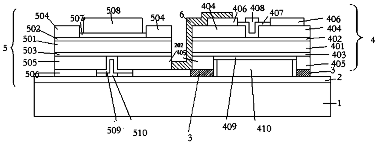
[0010] The invention provides a silicon-based InGaAs channel double-gate CMOS device, such as figure 1 As shown, the device includes a silicon substrate 1, bonding media 2 and 3 on the silicon substrate 1, and InGaAs composed of an InGaAs channel NMOS device 4, an InGaAs channel PMOS device 5 and an interconnection metal 6. A channel double-...


PUM


Abstract

The invention provides a silicon-based InGaAs channel dual gate COMS device. According to the invention, the device integrates a silicon-based semiconductor material and an InGaAs channel dual gate CMOS device by using the medium bonding method so as to increase the level of heterogeneous integration of the CMOS device. The dual gate structure also achieves reduction in power consumption of the device. The device makes it easy to adjust the threshold voltage thereof.

Description

technical field [0001] The invention relates to the technical field of semiconductors, in particular to a silicon-based InGaAs channel double-gate CMOS device. Background technique [0002] Since the development of integrated circuits, hundreds of millions of transistors can be integrated on silicon wafers. The power consumption and thermal effect of a single device have become the key factors restricting the development of integrated circuits. Integrating CMOS devices on silicon-based semiconductors has become a current research focus and technology frontier. However, the current InGaAs CMOS devices face two major problems: 1) heterogeneous integration of InGaAs CMOS devices and silicon substrates; 2) power consumption of CMOS devices after integration. To this end, it is necessary to improve the heterogeneous integration of InGaAs CMOS devices and silicon substrates, and to achieve low power consumption performance of the devices. Contents of the invention [0003] The...

Claims


Application Information

Patent Timeline
Patent Type & Authority Patents(China)
IPC IPC(8): H01L27/092H01L29/10H01L21/20
CPCH01L21/2007H01L27/0922H01L29/1079
Inventor 常虎东刘洪刚夏庆贞孙兵王盛凯
Owner INST OF MICROELECTRONICS CHINESE ACAD OF SCI
Features
  • R&D
  • Intellectual Property
  • Life Sciences
  • Materials
  • Tech Scout
  • Unparalleled Data Quality
  • Higher Quality Content
  • 60% Fewer Hallucinations
Learn More