Light emitting element

A light-emitting device, conductive type technology, applied in electrical components, semiconductor devices, electrical solid devices, etc., can solve the problems of current crowding, LED leakage and efficiency reduction, to prevent current crowding, good reliability, and improve current diffusion. The effect of efficiency

Active Publication Date: 2017-05-10
SEOUL VIOSYS CO LTD
View PDF4 Cites 2 Cited by
  • Summary
  • Abstract
  • Description
  • Claims
  • Application Information

AI Technical Summary

Problems solved by technology

Therefore, current does not diffuse efficiently in the p-type semiconductor layer, thereby causing current crowding in a certain region of the semiconductor layer
When current crowding occurs in the semiconductor layer, LEDs become susceptible to electrostatic discharge and can suffer from leakage and reduced efficiency

Method used


Image

  • Light emitting element
  • Light emitting element
  • Light emitting element

Examples


Embodiment Construction

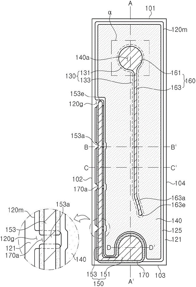
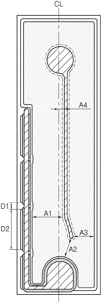
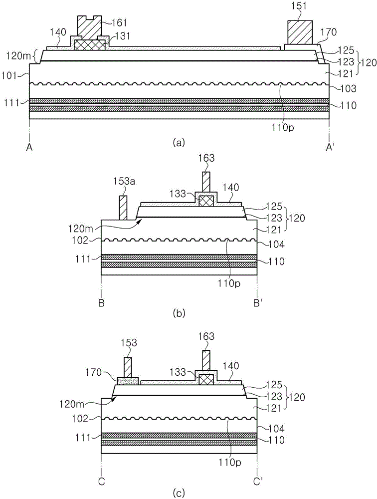
[0045]Hereinafter, exemplary embodiments of the present disclosure will be described in detail with reference to the accompanying drawings. The following embodiments are provided by way of examples in order to fully convey the spirit of the present disclosure to those skilled in the art to which the present disclosure pertains. Therefore, the present disclosure is not limited to the embodiments disclosed herein and can also be implemented in various forms. In the drawings, widths, lengths, thicknesses, etc. of elements may be exaggerated for clarity and descriptive purposes. When an element is referred to as being "disposed on" or "disposed on" another element, it can be directly "disposed on" or "disposed on" another element or intervening elements may be present. . Throughout the specification, the same reference numerals denote the same elements having the same or similar functions.

[0046] In the following, reference will be made to Figure 1a to Figure 9 A light emit...


PUM

PropertyMeasurementUnit
surface roughnessaaaaaaaaaa

Abstract

Disclosed is a light emitting element. The light emitting element comprises: a first conductive type semiconductor layer; a mesa that includes an active layer and a second conductive type semiconductor layer; a current blocking layer; a transparent electrode at least partially covering the current blocking layer; a first electrode that includes a first electrode pad and a first electrode extension; a second electrode that includes a second electrode pad and a second electrode extension; and an insulation layer partially located on the lower portion of the first electrode, wherein the mesa includes at least one groove formed on a side thereof, the first conductive type semiconductor layer is partially exposed through the groove, the insulation layer includes an opening through which the exposed first conductive type semiconductor layer is at least partially exposed, the first electrode extension includes one or more extension contact portions that are brought into contact with the first conductive type semiconductor layer through an opening, and the second electrode extension includes an end that has a width different from the average width of the second electrode extension.

Description

technical field [0001] Exemplary embodiments of the present disclosure relate to a light emitting device, and more particularly, to a light emitting device having high current spreading efficiency to provide good properties in terms of luminous efficiency and reliability. Background technique [0002] In general, a light emitting device such as a light emitting diode includes an n-type semiconductor layer that supplies electrons, a p-type semiconductor layer that supplies holes, and an active layer interposed between the n-type semiconductor layer and the p-type semiconductor layer. N-type and p-type electrodes are respectively formed on the n-type semiconductor layer and the p-type semiconductor layer to receive electric power from an external power source. [0003] On the other hand, a p-type semiconductor layer based on a nitride semiconductor has lower conductivity than an n-type semiconductor layer. Therefore, current does not diffuse efficiently in the p-type semicond...

Claims


Application Information

Patent Timeline
Patent Type & Authority Applications(China)
IPC IPC(8): H01L33/36
CPCH01L24/05H01L24/48H01L2224/48091H01L2224/48453H01L2224/48465H01L2924/00014H01L33/145H01L33/38H01L33/42H01L2224/05599H01L2224/45099H01L2224/85399H01L33/12H01L33/22H01L33/24H01L33/382H01L33/387
Inventor 徐德壹金艺瑟金京完禹尙沅金智惠
Owner SEOUL VIOSYS CO LTD
Why Eureka
Try Eureka