Semiconductor structure and formation method thereof

A technology of semiconductor and gate structure, applied in the field of semiconductor structure and its formation, can solve the problem that the electrical performance of the semiconductor structure needs to be improved, and achieve the effects of improving the electrical performance, increasing the driving current and reducing the contact resistance.

Active Publication Date: 2018-10-09
SEMICON MFG INT (SHANGHAI) CORP +1
View PDF6 Cites 0 Cited by
  • Summary
  • Abstract
  • Description
  • Claims
  • Application Information

AI Technical Summary

Problems solved by technology

[0006] However, the electrical performance of the formed semiconductor structur

Method used


Image

  • Semiconductor structure and formation method thereof
  • Semiconductor structure and formation method thereof
  • Semiconductor structure and formation method thereof

Examples


Embodiment Construction

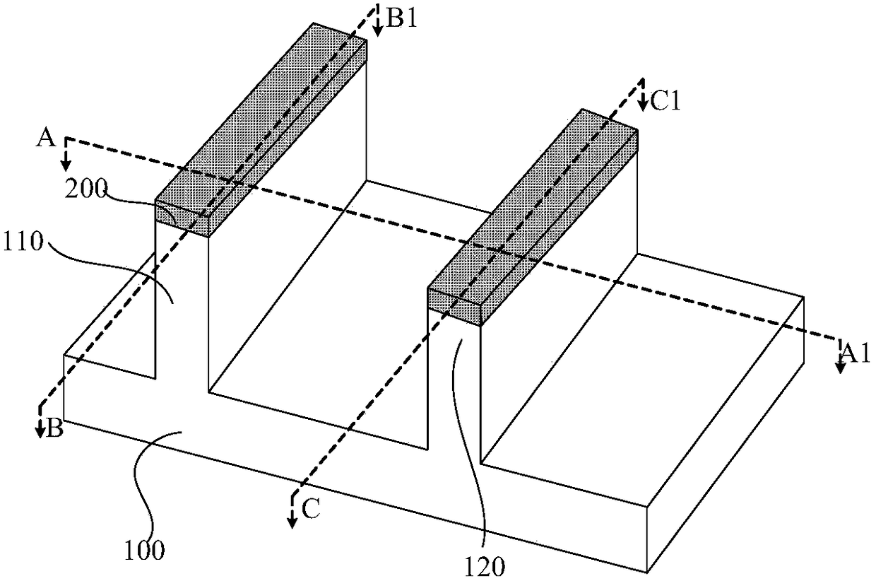
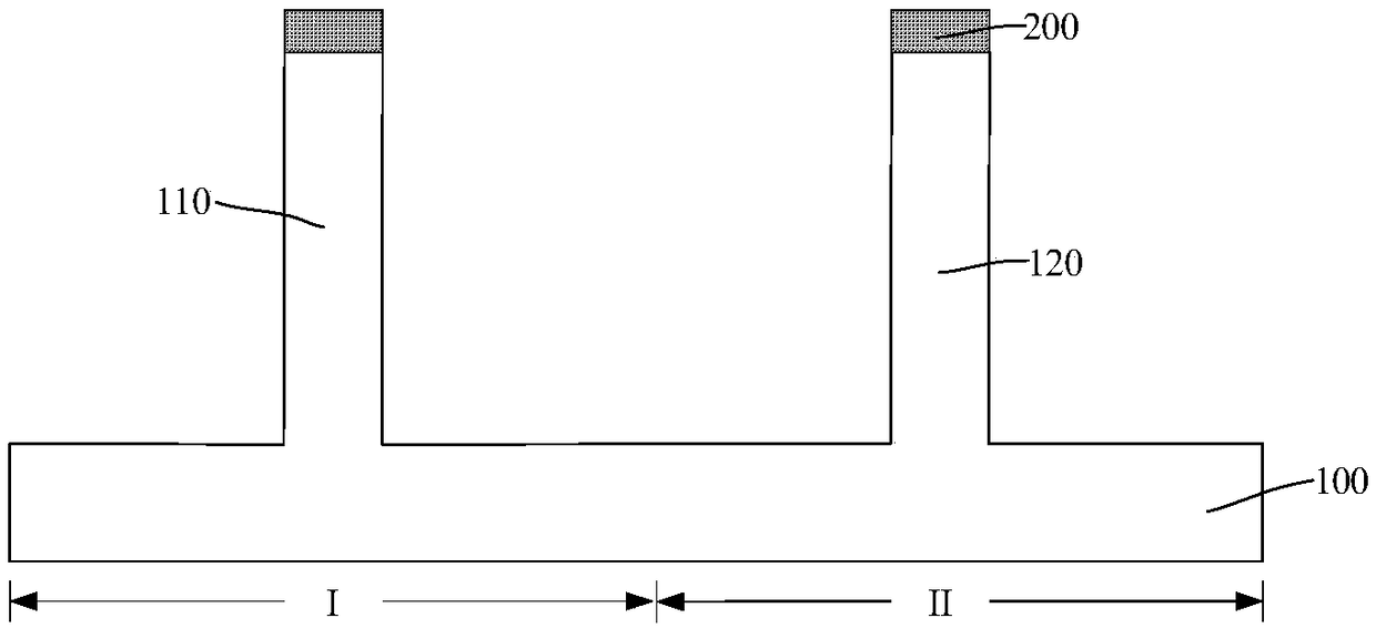
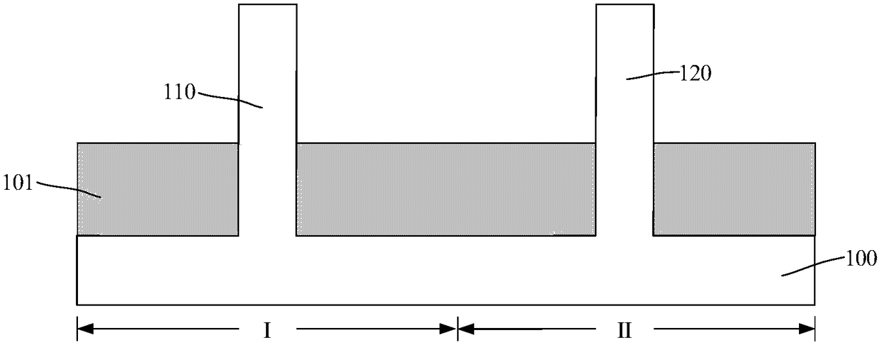
[0016] The parasitic external resistance (Rext) is an important factor affecting the electrical performance of semiconductor structures; among them, the parasitic external resistance is mainly affected by the contact resistance ((ρc) between the contact hole plug and the source-drain doped region. Therefore, in order to reduce The main way to reduce the contact resistance to increase the driving current is to form a metal silicide layer on the surface of the substrate corresponding to the position where the contact hole plug is to be formed, so as to reduce the contact resistance of the contact area.

[0017] However, even after adopting the metal silicide layer technology, the electrical performance of the formed semiconductor structure still needs to be improved.

[0018] In order to solve the above technical problem, the present invention provides a method for forming a semiconductor structure, comprising: forming N-region grooves in the substrate on both sides of the NMOS r...


PUM

PropertyMeasurementUnit
Doping concentrationaaaaaaaaaa
Thicknessaaaaaaaaaa

Abstract

A semiconductor structure and a formation method thereof are disclosed. The method comprises the following steps of providing a substrate including an NMOS area; forming a gate structure on the substrate; forming an N-region groove in the substrate of the two sides of the gate structure; forming an N-region doped epitaxial layer in an N-region groove, wherein the N-region doped epitaxial layer isthe laminated structure of a first N-type doped epitaxial layer and a second N-type doped epitaxial layer, the first N-type doped epitaxial layer is a first epitaxial layer doped with N-type ions, thesecond N-type doped epitaxial layer is a second epitaxial layer doped with the N-type ions, and the forbidden band width of the second epitaxial layer is smaller than the forbidden band width of thefirst epitaxial layer; forming an interlayer dielectric layer on the N-region doped epitaxial layer; forming a first contact opening which is exposed out of the N-region doped epitaxial layer in the interlayer dielectric layer; and forming a first contact hole plug in the first contact opening. In the invention, through the second epitaxial layer doped with the N-type ions, a Schottky barrier height is reduced, the N-type ion concentration of the N-region doped epitaxial layer is increased and a contact resistance is reduced.

Description

technical field [0001] The invention relates to the field of semiconductors, in particular to a semiconductor structure and a forming method thereof. Background technique [0002] With the continuous development of integrated circuit manufacturing technology, people's requirements for the integration and performance of integrated circuits are becoming higher and higher. In order to improve integration and reduce costs, the critical dimensions of components are getting smaller and the circuit density inside integrated circuits is increasing. This development makes the surface of the wafer unable to provide enough area to make the required interconnection lines. [0003] In order to meet the requirements of the interconnection line after the critical dimension is reduced, at present, the conduction between different metal layers or between the metal layer and the substrate is realized through the interconnection structure. The interconnection structure includes interconnectio...

Claims


Application Information

Patent Timeline
IPC IPC(8): H01L27/092
CPCH01L21/77H01L27/0928
Inventor 李勇
Owner SEMICON MFG INT (SHANGHAI) CORP
Why Eureka
Try Eureka