

Laser-Based Control of Surface Morphology of Nanostructured Silicon Substrates
A nanostructure and surface morphology technology, applied in the process of producing decorative surface effects, manufacturing microstructure devices, nanotechnology, etc., can solve the problem of affecting surface morphology, distortion of silicon-based surface morphology, and unsatisfactory silicon-based surface morphology and other problems, to achieve the effect of short time and high efficiency
- Summary
- Abstract
- Description
- Claims
- Application Information
AI Technical Summary
Problems solved by technology
Method used
Image

Examples
Embodiment 1
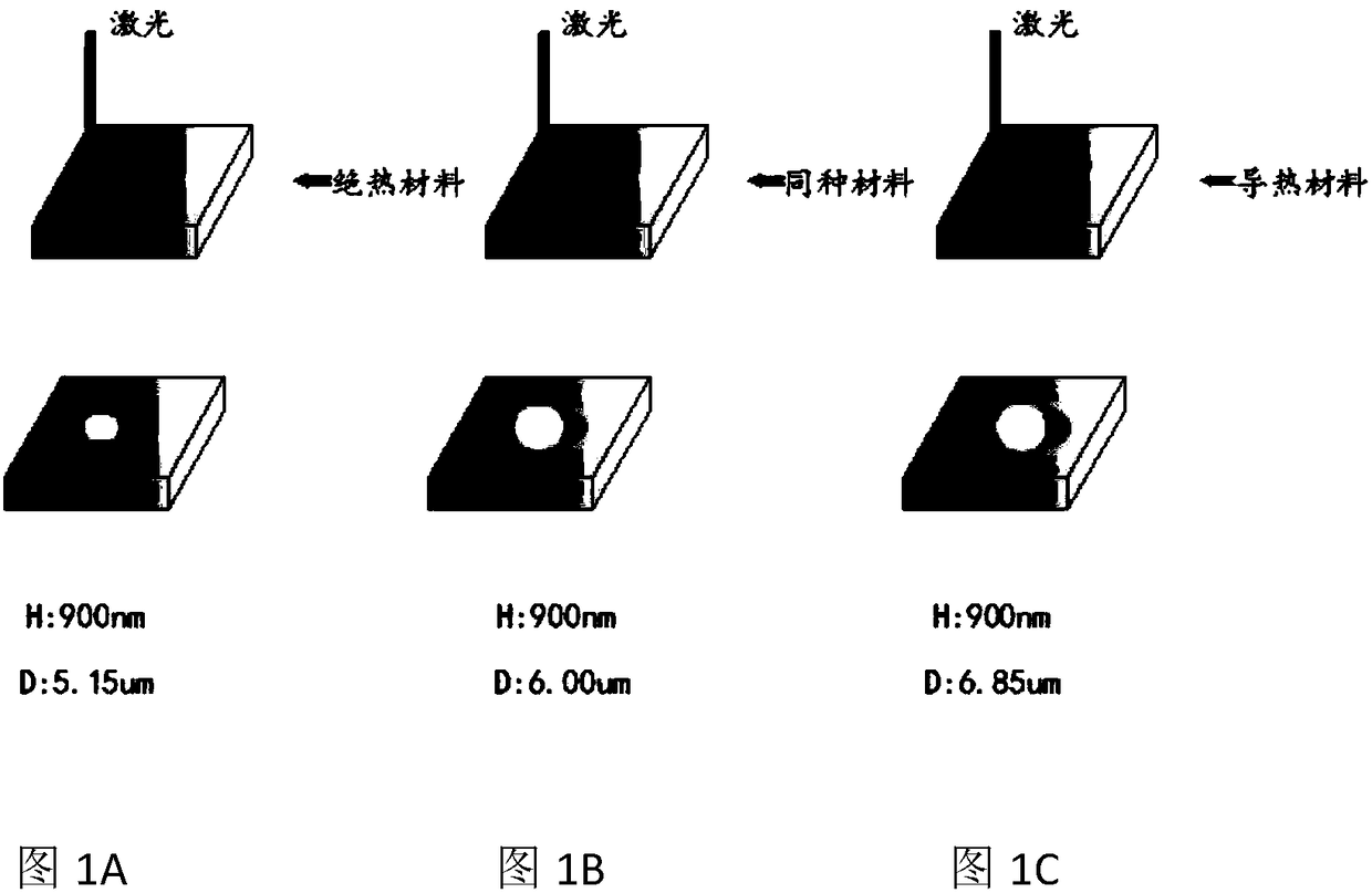
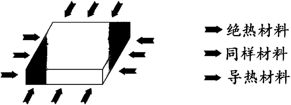
[0036] Use asbestos (thermal insulation material) to touch the right plane of the nanostructure silicon substrate, the thermal conductivity of asbestos k 1 =0W / m-K. Then adjust the power of the laser to P=75mW, and irradiate the surface of the silicon-based material for 10 seconds. After laser irradiation, the silicon substrate was placed under an optical magnifying instrument for observation. The result of observation is that there is a raised silicon-based surface morphology in the center of the silicon substrate, and the corresponding height H=900nm and maximum diameter D=5.15um are measured, and the corresponding aspect ratio is 0.175, as Figure 1A shown.
Embodiment 2
[0038] Use silicon (the same material) to contact the right plane of the nanostructured silicon substrate, the thermal conductivity of silicon k 2 = 150W / m-K. Repeat the above operations to measure the corresponding height H = 900nm and the largest diameter D = 6.00um, the corresponding aspect ratio is 0.150, such as Figure 1B shown.
Embodiment 3
[0040] Use aluminum (thermal conductive material) to contact the right plane of the nanostructure silicon substrate, the thermal conductivity of aluminum k 3 = 200W / m-K. Repeat the above operations to measure the corresponding height H=900nm and maximum diameter D=6.85um, and the corresponding aspect ratio is 0.131, such as Figure 1C shown.
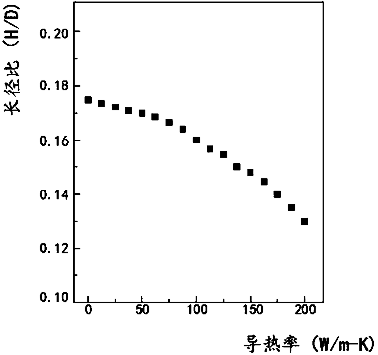
[0041] It can be seen from the above examples that when the thermal conductivity of the contact material gradually increases (the thermal conductivity of asbestos is the lowest, the thermal conductivity of silicon is medium, and the thermal conductivity of aluminum is the highest), the maximum height of the silicon-based surface morphology will not change. The maximum diameter D becomes larger and larger. According to the aspect ratio of the maximum height H / maximum diameter D, it can be obtained that the aspect ratio of the silicon-based surface morphology is getting smaller and smaller.
[0042] The above is to study the aspect rati...
PUM
| Property | Measurement | Unit |
|---|---|---|
| height | aaaaa | aaaaa |
| aspect ratio | aaaaa | aaaaa |
| aspect ratio | aaaaa | aaaaa |
Abstract
Description
Claims
Application Information