Sensor pixel and optical sensor

A technology of sensor pixels and photosensitive elements, applied in instruments, character and pattern recognition, computer components, etc., can solve the problem of low image quality and achieve the effect of improving image quality and signal-to-noise ratio

Pending Publication Date: 2018-01-09
MICROARRAY MICROELECTRONICS CORP LTD
View PDF0 Cites 16 Cited by
  • Summary
  • Abstract
  • Description
  • Claims
  • Application Information

AI Technical Summary

Problems solved by technology

[0005] The invention provides a sensor pixel and an optical sensor to solve the problem of low image quality caused by overexposure or underexposure, realize dynamic adjustm

Method used


Image

  • Sensor pixel and optical sensor
  • Sensor pixel and optical sensor
  • Sensor pixel and optical sensor

Examples


Embodiment Construction

[0042] The present invention will be further described in detail below in conjunction with the accompanying drawings and embodiments. It should be understood that the specific embodiments described here are only used to explain the present invention, but not to limit the present invention. In addition, it should be noted that, for the convenience of description, only some structures related to the present invention are shown in the drawings but not all structures. The present invention uses a fingerprint sensor as an example to explain the working principle of the integral adjustment circuit, but does not limit the protection scope of the present invention, and the protection scope of the present invention should be based on the contents of the claims.

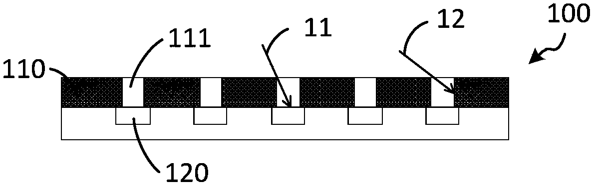
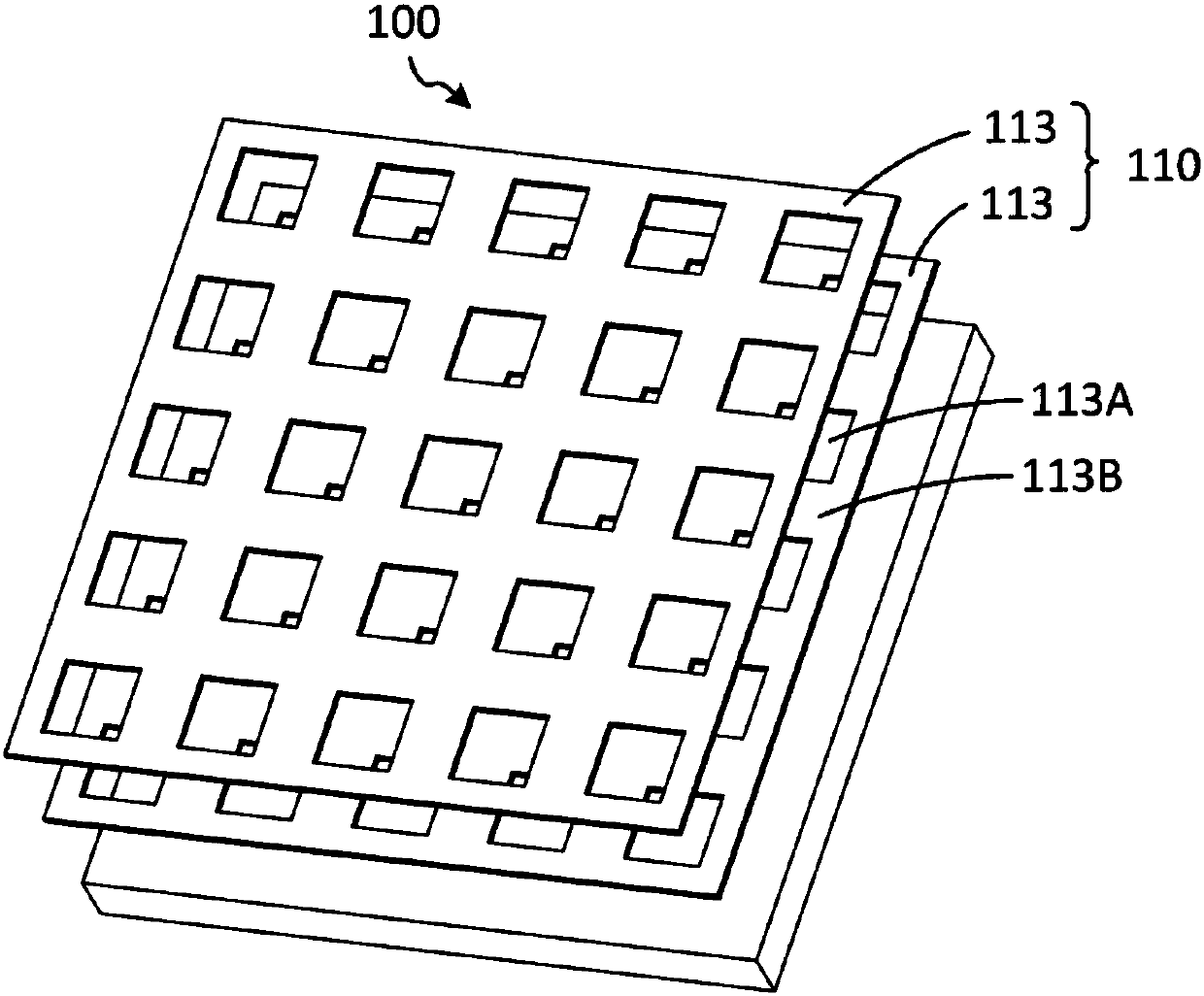
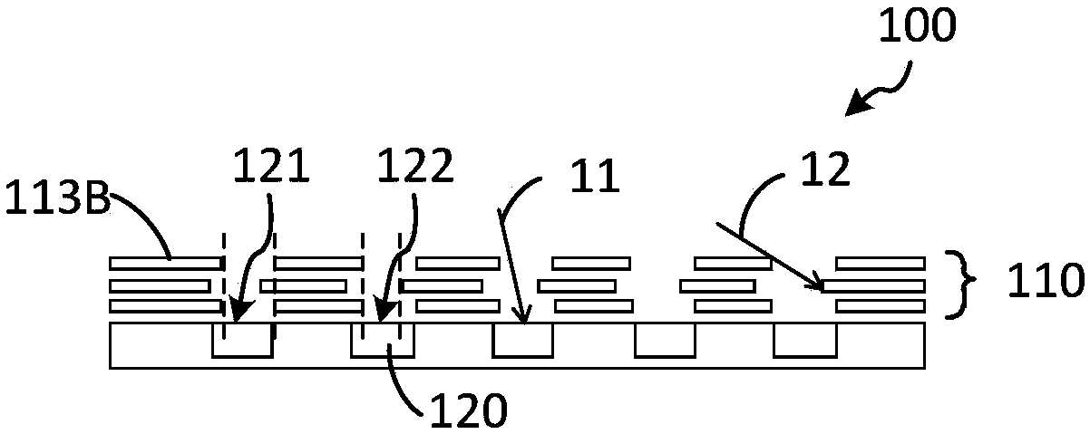
[0043] figure 1 A schematic cross-sectional view of a sensor pixel provided by an embodiment of the present invention, the specific structure of the sensor pixel 100 is as follows:

[0044] A collimation layer 110, an optica...


PUM


Abstract

An embodiment of the present invention discloses a sensor pixel and an optical sensor, wherein the sensor pixel includes: a collimation layer, an optical tunnel is formed in the collimation layer, and the optical tunnel is used for receiving light reflected by a target finger in a substantially vertical direction. direction of light; at least two photosensitive elements for outputting electrical signals according to the light received by the optical tunnel; a signal detection circuit, electrically connected to one or more of the photosensitive elements, for acquiring the gated photosensitive elements The output electrical signal; the control unit is used to control the number of the photosensitive element gates. The technical solution provided by the embodiments of the present invention solves the problem of low quality of fingerprint images caused by overexposure or underexposure, and realizes the dynamic adjustment of the electronic aperture size of the sensor pixels, that is, realizes the dynamic adjustment of the exposure of the sensor pixels, so that the Get better image quality and improve the effect of signal-to-noise ratio.

Description

technical field [0001] Embodiments of the present invention relate to fingerprint identification technology, and in particular to a sensor pixel and an optical sensor. Background technique [0002] Fingerprint sensors are currently mainly divided into two categories, namely optical fingerprint sensors and capacitive fingerprint sensors. The capacitive fingerprint sensor images the fingerprint by measuring the difference in the connection capacitance formed between the fingerprint valley line, the ridge line and the planar sensing electrode array unit. When the dielectric layer between the sensing electrode array and the finger is thicker, the capacitance will attenuate, and the image of the sensor will be blurred. Due to the development of technology, the thickness of the dielectric layer between the sensing electrode and the target electrode of the fingerprint sensor has increased from the order of 10um to the order of 100um. What's more, considering the integrity of the ...

Claims


Application Information

Patent Timeline
IPC IPC(8): G06K9/00
Inventor 李扬渊
Owner MICROARRAY MICROELECTRONICS CORP LTD
Why Eureka
Try Eureka