Active component substrate

A technology of active components and substrates, applied in electrical components, electric solid-state devices, semiconductor devices, etc., can solve the problem of poor display, difficult alignment of the film layer belonging to the scanning line and the film layer belonging to the transparent electrode, and the wrong edge of the measurement system. video, etc.

Active Publication Date: 2018-01-12
AU OPTRONICS CORP
View PDF9 Cites 0 Cited by
  • Summary
  • Abstract
  • Description
  • Claims
  • Application Information

AI Technical Summary

Problems solved by technology

However, under high frequency (for example: 144Hz) driving, if the RC loading of the display panel is too high, poor display is likely to occur
In view of this, the design of the scanning lines of the display panel can be changed to reduce the resistive capacitance load, but when the design of the scanning lines is changed, the edge of the film layer to which the scan line belongs is too close to the edge of the film layer to which the transparent electrode belongs, and the measurement system is prone to errors The wrong edge image is taken, which makes it difficult to judge the alignment of the film layer to which the scan line belongs and the film layer to which the transparent electrode belongs

Method used


Image

  • Active component substrate
  • Active component substrate
  • Active component substrate

Examples


Embodiment Construction

[0056] The technical solution of the present invention will be described in detail below in conjunction with the accompanying drawings and specific embodiments to further understand the purpose, solution and effect of the present invention, but it is not intended to limit the scope of protection of the appended claims of the present invention.

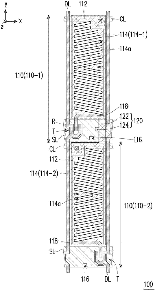
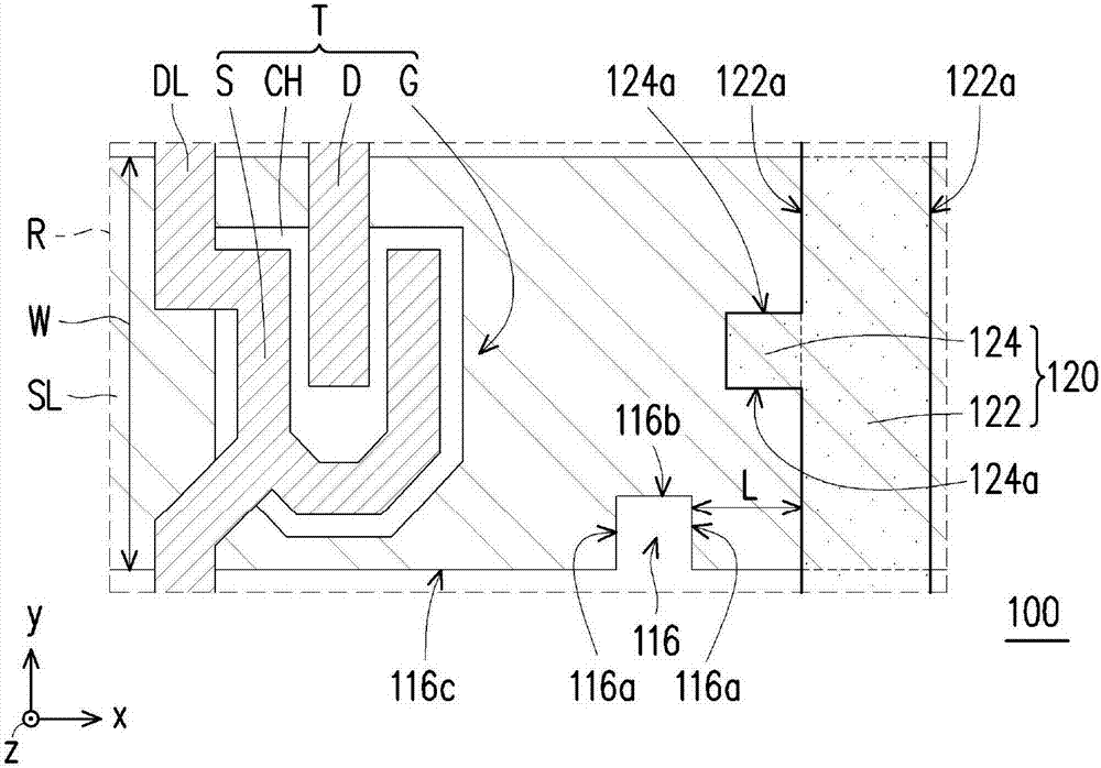
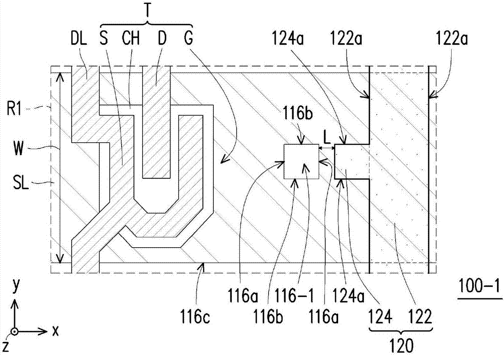
[0057] figure 1 It is a schematic top view of an active device substrate according to an embodiment of the present invention. figure 2 for figure 1 An enlarged schematic view of a part R of the active device substrate 100 of FIG. Please refer to figure 1 and figure 2 , the active device substrate 100 includes a plurality of pixel units 110 and a preset pattern 120 . A plurality of pixel units 110 and a predetermined pattern 120 are disposed on a substrate (not shown). The base is mainly a component for supporting the active device substrate 100 . In this embodiment, the material of the substrate can be glass, quartz, organic po...


PUM


Abstract

An active component substrate includes a plurality of pixel units and a predetermined pattern. Each of the pixel units includes a scan line extending along a first direction, a data line crossing thescan line, a pixel electrode electrically connected with the scan line and the data line, and a common electrode overlapping the pixel electrode. The scan line of at least one pixel unit has a presetopening. The predetermined pattern belongs to the same layer as the common electrode. The predetermined pattern is disposed on the scan line of at least one pixel unit. The predetermined pattern has aplurality of first side edges and an opposite second side edge. The first sides and the second side are located within the area of the scan line. The first sides are perpendicular to the first direction, and the second side is parallel to the first direction.

Description

technical field [0001] The present invention relates to a substrate, and in particular to an active component substrate. Background technique [0002] With the advancement of display technology, the resolution of display panels continues to increase. Generally speaking, today's display panels have sufficient high resolution, and consumers' attention to display panel specifications is no longer limited to this. In detail, consumers are more concerned about the display fluency of dynamic images. Generally speaking, in order to display dynamic images smoothly, the frame rate of the display panel can be increased. For example, the refresh rate of the display panel can be increased from the usual 60Hz to 144Hz. However, under high-frequency (for example: 144Hz) driving, if the RC loading of the display panel is too high, poor display is likely to occur. In view of this, the design of the scanning lines of the display panel can be changed to reduce the resistive capacitance lo...

Claims


Application Information

Patent Timeline
IPC IPC(8): H01L27/12H01L21/66G02F1/1362
Inventor 江逸凡
Owner AU OPTRONICS CORP
Why Eureka
Try Eureka