Semiconductor light-emitting chip, semiconductor light-emitting module, display device and terminal equipment

A light-emitting chip and light-emitting module technology, which is applied in the direction of semiconductor devices, electric solid-state devices, electrical components, etc., can solve problems that restrict the development and application of semiconductor light-emitting chips

Inactive Publication Date: 2018-01-26
HUAWEI TECH CO LTD
View PDF4 Cites 4 Cited by
  • Summary
  • Abstract
  • Description
  • Claims
  • Application Information

AI Technical Summary

Problems solved by technology

Therefore, the existing semiconductor light-emitting chips cannot meet the above requirements, which seriously restricts the development and application of semiconductor light-emitting chips.

Method used


Image

  • Semiconductor light-emitting chip, semiconductor light-emitting module, display device and terminal equipment
  • Semiconductor light-emitting chip, semiconductor light-emitting module, display device and terminal equipment
  • Semiconductor light-emitting chip, semiconductor light-emitting module, display device and terminal equipment

Examples


Embodiment Construction

[0059] The technical solution in this application will be described below with reference to the accompanying drawings.

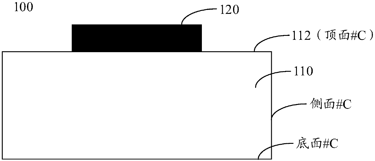
[0060] figure 1 is a schematic front view of a semiconductor light emitting chip according to an embodiment of the present invention, figure 2 is a schematic front view of a semiconductor light emitting chip according to an embodiment of the present invention.

[0061] Such as figure 1 or figure 2 As shown, the semiconductor light emitting chip 100 of the embodiment of the present invention includes a chip body 110 and a light distribution adjusting layer 120 .

[0062] Next, the structure and functions of the chip main body 110 will be described first.

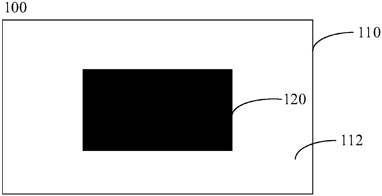
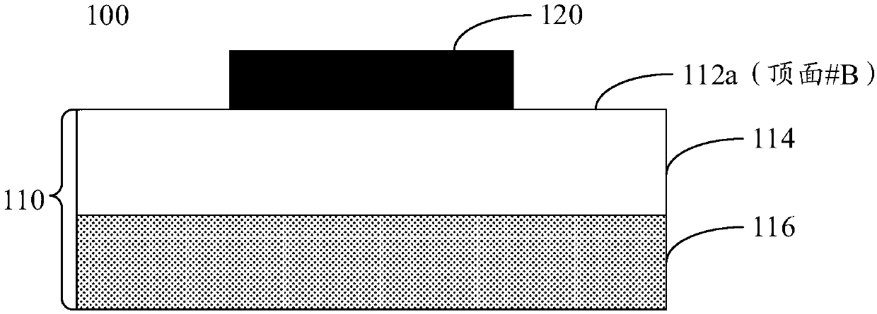
[0063] image 3 An example of the configuration of the chip body 110 according to the embodiment of the present invention is shown, Figure 4 Another example of the chip body 110 of the embodiment of the present invention is shown.

[0064] Such as image 3 or Figure 4 As shown, in the embodimen...


PUM


Abstract

The invention provides a semiconductor light-emitting chip, a semiconductor light-emitting module, a display device and terminal equipment. The semiconductor light-emitting chip comprises a chip mainbody and a light distribution adjustment layer, wherein the chip main body comprises a first surface and a plurality of side surfaces; the first surface is intersected with the side surfaces; the light distribution adjustment layer covers the first surface and extends along the thickness direction of the chip main body; a projection of the light distribution adjustment layer on the first surface is located in the first surface or the light distribution adjustment layer covers at least one side surface; the light distribution adjustment layer partially or completely covers the area of each sidesurface; and the light distribution adjustment layer can partially or completely reflect the light entering the light distribution adjustment layer.

Description

technical field [0001] The present application relates to the field of semiconductors, and more specifically, to semiconductor light emitting chips, semiconductor light emitting modules, display devices and terminal equipment. Background technique [0002] At present, there is known a semiconductor light-emitting chip, which is composed of a semiconductor layer capable of emitting light and a substrate for forming (or growing) the semiconductor layer. [0003] In the prior art, the distribution of the light emitted by the semiconductor chip (or in other words, the intensity of the light emitted by the semiconductor chip in each irradiation direction) is fixed. [0004] With the development and progress of display technology, for example, when semiconductor light-emitting chips are applied to backlight sources such as liquid crystal displays, in order to ensure uniform light distribution, it is hoped that the distribution of light emitted by the semiconductor chip can be chan...

Claims


Application Information

Patent Timeline
Patent Type & Authority Applications(China)
IPC IPC(8): H01L33/46H01L33/00H01L25/075
Inventor 曲爽欧阳世宏刘康仲
Owner HUAWEI TECH CO LTD
Why Eureka
Try Eureka