Eureka AIR delivers breakthrough ideas for toughest innovation challenges, trusted by R&D personnel around the world.

Semiconductor process conveying system and method

A conveying system and semiconductor technology, applied in semiconductor/solid-state device manufacturing, conveyor objects, transportation and packaging, etc., can solve the problems of increased plant investment and cost, and achieve the effect of avoiding repeated operations

Inactive Publication Date: 2018-07-06
FITTECH
View PDF4 Cites 2 Cited by
  • Summary
  • Abstract
  • Description
  • Claims
  • Application Information

AI Technical Summary

Problems solved by technology

However, the known delivery trolley can only transport the pods to the machines on the same side and facing in the same direction. When a plurality of machines are located on different sides or facing in different directions, another matching one must be additionally provided. Only the transport trolley can smoothly transport the pods, which will greatly increase the cost of the plant investment and increase the plant area, and there are shortcomings that need to be improved urgently

Method used


Image

  • Semiconductor process conveying system and method
  • Semiconductor process conveying system and method
  • Semiconductor process conveying system and method

Examples


Embodiment Construction

[0022] The following examples only illustrate possible embodiments of the present invention, which are not intended to limit the protection scope of the present invention, and are stated in advance.

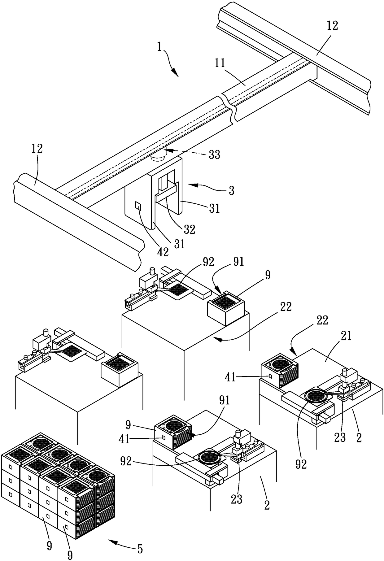
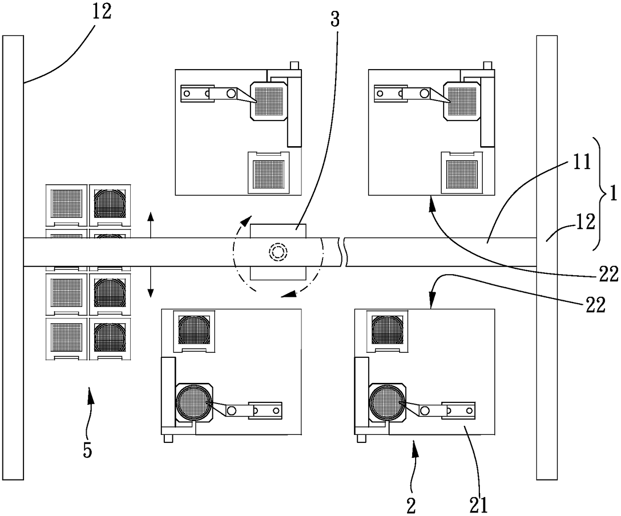
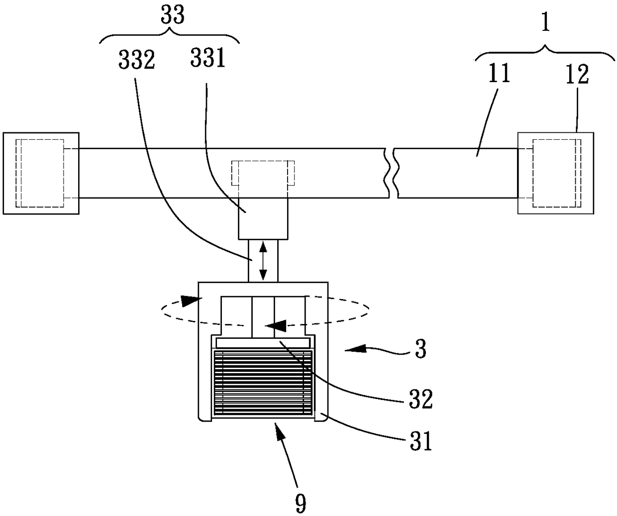
[0023] Please refer to Figures 1 to 3 , which shows a preferred embodiment of the present invention, the semiconductor process delivery system and method of the present invention includes a displacement mechanism 1 , a plurality of machines 2 and a pick-up mechanism 3 .

[0024] The displacement mechanism 1 includes a first track 11 extending along a first direction.

[0025] A plurality of machines 2 are respectively arranged on both sides of the first track 11, each machine 2 has a working platform 21, the working platform 21 is for placing at least one pod 9, and each pod 9 is for accommodating at least one wafer 92 , each working platform 21 has a feeding end 22 adjacent to and facing the first track 11 .

[0026] The taking mechanism 3 can be movably arranged on the first...


PUM


Abstract

The invention provides a semiconductor process conveying system and method, and the system comprises a displacement mechanism, a plurality of platforms, and a taking mechanism. The displacement mechanism comprises a first track which extends in a first direction. The plurality of platforms are respectively disposed at two sides of the first rack, and each platform is provided with a working platform which is used for placing at least one crystal cup box. The taking mechanism is movably disposed on the first track, and can take one crystal cup box from one working platform or placing one crystal cup box on one working platform. Moreover, the invention provides a conveying method employing the above structure. The system and method provided by the invention can enable the crystal cup boxes to be successfully placed on the platforms located at two sides of the taking mechanism or to successfully take the crystal cup boxes from the platforms located at two sides of the taking mechanism.

Description

technical field [0001] The invention relates to a semiconductor manufacturing process conveying system and method. Background technique [0002] Generally, in the semiconductor manufacturing process, after the wafer is manufactured, it needs to be transported to be inspected or marked, so as to eliminate the bad chips in the wafer. In order to facilitate the transport of the wafer, the known technology is to stack multiple wafers on the A pod, and a transport trolley transports the pod from the concentration area to the machine, and after the inspection or marking operation is completed, it is transported back to the concentration area for the next station operation. However, the known delivery trolley can only transport the pods to the machines on the same side and facing in the same direction. When a plurality of machines are located on different sides or facing in different directions, another matching one must be additionally provided. Only the transport trolley can smo...

Claims


Application Information

Patent Timeline
Patent Type & Authority Applications(China)
IPC IPC(8): H01L21/677
CPCH01L21/67703H01L21/67706H01L21/67736
Inventor 林奕良陈世颖陈宏沛
Owner FITTECH
Why Eureka
Eureka Blog
Learn More