Miniature light-emitting component and manufacturing method thereof

A technology of light-emitting elements and manufacturing methods, which is applied in the direction of electrical elements, electric solid-state devices, semiconductor devices, etc., and can solve problems such as prone to broken bridges and dropped electrodes

Active Publication Date: 2018-08-17
XIAMEN SANAN OPTOELECTRONICS TECH CO LTD
View PDF7 Cites 35 Cited by
  • Summary
  • Abstract
  • Description
  • Claims
  • Application Information

AI Technical Summary

Problems solved by technology

In order to achieve mass transfer, the chip is made in the air, and the corresponding bridge test is required, but it is prone to problems such as broken bridges or peeling.

Method used


Image

  • Miniature light-emitting component and manufacturing method thereof
  • Miniature light-emitting component and manufacturing method thereof
  • Miniature light-emitting component and manufacturing method thereof

Examples


specific Embodiment

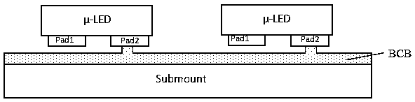
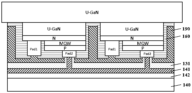
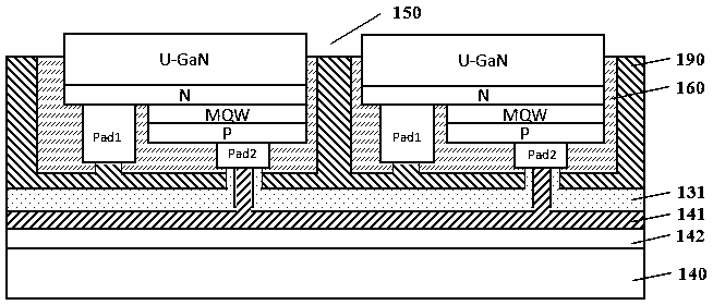
[0052] image 3(a) is the pattern on the lower surface of the micro light emitting diode chip in the first preferred embodiment. The micro light emitting diode includes: an epitaxial stack layer, which sequentially includes a first type semiconductor layer, an active layer, and a second type semiconductor layer. having opposite first and second surfaces; a first electrode formed on the second surface of the epitaxial stack and connected to the first type semiconductor layer; a second electrode formed on the epitaxial stack On the second surface of the second electrode, it is connected with the second type semiconductor layer; the first electrode is divided into a first region 121a, a second region 131a and a third region 141a from the inside to the outside at the center of the electrode, and the three Regions can be distinguished by surface topography or appearance color. The LED chip 110 is a thin-film microstructure, and its preferred size is within 100 μm×100 μm, such as 1...


PUM


Abstract

The invention discloses a miniature light-emitting component and a manufacturing method thereof. A support pillar of a pinhole electrode is formed by a conductive substrate and insulation isolation, and a common-electrode parallel connection is used. A modular metal sacrificial layer is used as a test electrode to realize a huge amount of measurement of the miniature light-emitting component. Theminiature light-emitting component comprises: an epitaxial stack successively comprising a first type of semiconductor layer, an active layer, a second type of semiconductor layer and having oppositefirst and second surfaces; a first electrode formed on the second surface on the epitaxial stack and connected to the first type of semiconductor layer; a second electrode formed on the second surfaceof the epitaxial stack and connected to the second type of semiconductor layer; and first connection regions disposed on the surface of the first electrode and the second electrode. The first connection regions can be distinguished from other regions of the electrode where it is located from the surface topography or appearance color.

Description

technical field [0001] The invention belongs to the field of semiconductor manufacturing, and in particular relates to a micro light-emitting element and a manufacturing method thereof. Background technique [0002] Micro LED (Micro LED, also known as μ-LED), in addition to OLED self-illumination, thin thickness, light weight, large viewing angle, short response time, high luminous efficiency, etc., it is easier to achieve high PPI (pixel density) and small size , easy to carry, low power consumption and other excellent characteristics, many units in the LED industry have devoted themselves to the development and application of components. Since the LED chip is very small and the electrode is smaller than the probe, how to realize the full test has become a very important difficulty. At present, it is mainly to sacrifice part of the chip to realize sampling test. In order to achieve mass transfer, the chip is manufactured in a floating type, and correspondingly, a floating...

Claims


Application Information

Patent Timeline
Patent Type & Authority Applications(China)
IPC IPC(8): H01L33/36H01L33/00
CPCH01L33/005H01L33/36G01R31/2635H01L2933/0033H01L33/62H01L2933/0066H01L33/44H01L2933/0025H01L25/0753G01R31/2884H01L2224/95136H01L24/95H01L33/0093H01L2933/0016
Inventor 钟志白李佳恩郑锦坚吴政徐宸科康俊勇
Owner XIAMEN SANAN OPTOELECTRONICS TECH CO LTD
Why Eureka
Try Eureka