
Electrostatic detection devices and methods thereof

一种静电检测、电子装置的技术,应用在测量装置、静电场测量、测量电变量等方向,能够解决难达到静电耐受度的规范、耗费大时间等问题

Active Publication Date: 2018-11-13
QUANTA COMPUTER INC
View PDF6 Cites 3 Cited by
  • Summary
  • Abstract
  • Description
  • Claims
  • Application Information

AI Technical Summary

Problems solved by technology

[0002] Today's electronic devices are becoming smaller and smaller as the size of the semiconductor process and users' requirements for portability make the printed circuit boards in electronic products smaller and smaller, and the electronic components on the printed circuit boards are denser. In addition, in order to meet more complex electronic functions, the high logic level and ground level inside the integrated circuit will become closer, making it more difficult for electronic products to meet the specifications for the tolerance of static electricity
[0003] However, for engineers, the biggest difficulty in improving the tolerance of static electricity is how to find the area of ​​the system that is disturbed by static electricity, which will consume a lot of time in the process of finding

Method used


Image

  • Electrostatic detection devices and methods thereof
  • Electrostatic detection devices and methods thereof
  • Electrostatic detection devices and methods thereof

Examples


Embodiment Construction

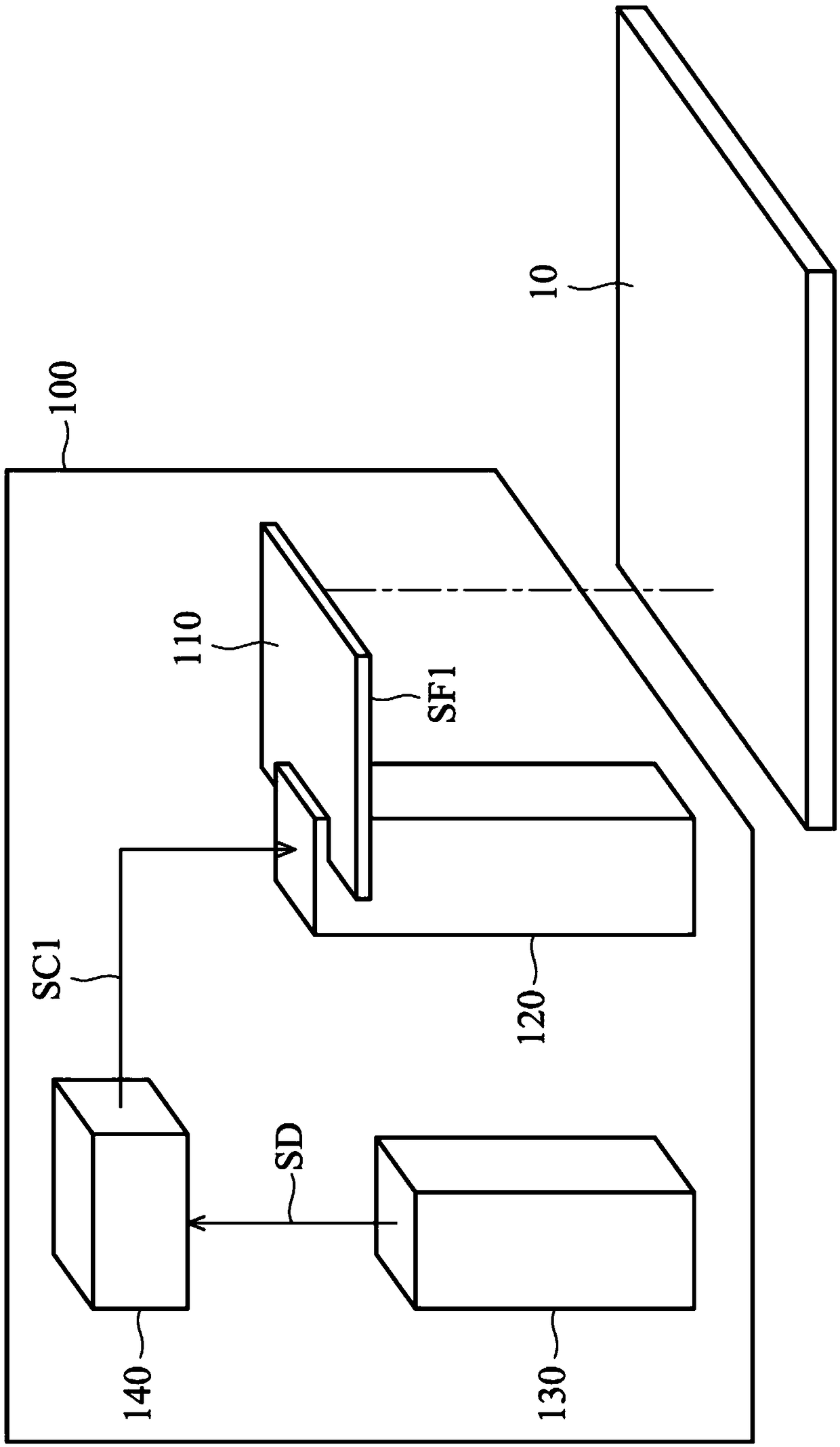
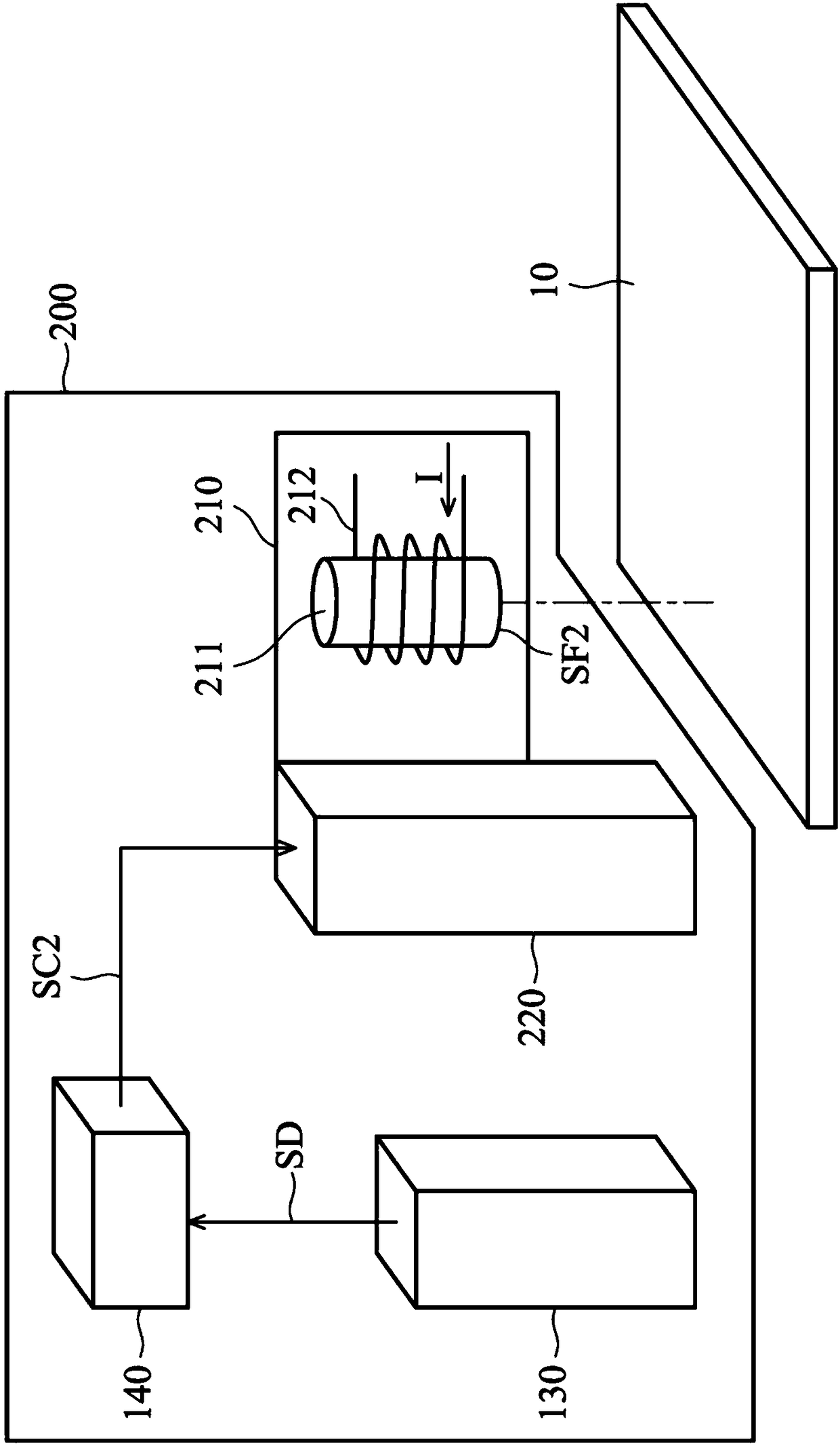
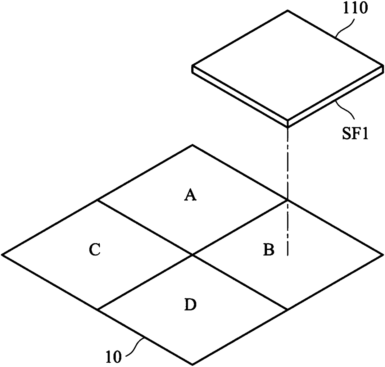
[0019] The following descriptions are examples of the present invention. Its purpose is to illustrate the general principle of the present invention, which should not be regarded as a limitation of the present invention, and the scope of the present invention should be defined by the claims.

[0020] It is worth noting that the following disclosure may provide multiple embodiments or examples for practicing different features of the present invention. The specific component examples and arrangements described below are only used to briefly illustrate the spirit of the present invention, and are not intended to limit the scope of the present invention. In addition, the following description may reuse the same component symbols or words in multiple examples. However, the purpose of repeated use is only to provide simplified and clear description, and is not intended to limit the relationship among multiple embodiments and / or configurations discussed below. In addition, descrip...


PUM


Abstract

An electrostatic detection device, which is configured to detect an electrostatically sensitive area of an electronic device causing a specific event to happen to an electronic device, includes an electrostatic metal plate, a detector, and a controller. The electrostatic metal plate is configured to generate an electrical field and includes a first surface which is parallel to the electronic device. When the specific event is detected, the detector generates a detection signal. The controller moves the first surface relative to the electronic device and receives the detection signal. When thedetection signal is received, the controller determines that the electrostatically sensitive area is a first area of the electronic device overlapped with the first surface.

Description

technical field [0001] The invention relates to a device and method for detecting electrostatic sensitive areas of electronic devices. Background technique [0002] Today's electronic devices are becoming smaller and smaller as the size of the semiconductor process and users' requirements for portability make the printed circuit boards in electronic products smaller and smaller, and the electronic components on the printed circuit boards are denser. In addition, in order to meet more complex electronic functions, the high logic level and the ground level inside the integrated circuit will become closer, making it more difficult for electronic products to meet the specifications for the tolerance to static electricity. [0003] However, for engineers, the biggest difficulty in improving the tolerance of static electricity is how to find the area of ​​the system that is disturbed by static electricity, which will consume a lot of time in the search process. Therefore, there i...

Claims


Application Information

Patent Timeline
Patent Type & Authority Applications(China)
IPC IPC(8): G01R29/12
CPCG01R29/12G01R31/002G01R29/24G01R15/165
Inventor 郭昭宏
Owner QUANTA COMPUTER INC
Learn More