Semiconductor structure and forming method thereof

A technology of semiconductor and device area, applied in the field of semiconductor structure and its formation, can solve problems such as performance degradation of semiconductor structure, and achieve the effects of improving performance, improving top recess, and improving top flatness

Active Publication Date: 2018-11-23
SEMICONDUCTOR MANUFACTURING INTERNATIONAL (BEIJING) CORP +1
View PDF5 Cites 0 Cited by
  • Summary
  • Abstract
  • Description
  • Claims
  • Application Information

AI Technical Summary

Problems solved by technology

[0005] However, the process of forming the metal resistive device tends to degrade the performance of the semiconductor structure

Method used


Image

  • Semiconductor structure and forming method thereof
  • Semiconductor structure and forming method thereof
  • Semiconductor structure and forming method thereof

Examples


Embodiment Construction

[0023] It can be seen from the background art that the process of forming the metal resistance device easily leads to performance degradation of the semiconductor structure. Analyzing the performance degradation of the semiconductor structure due to:

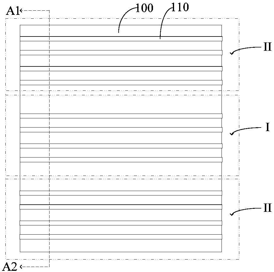
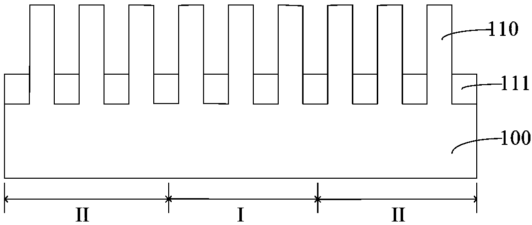
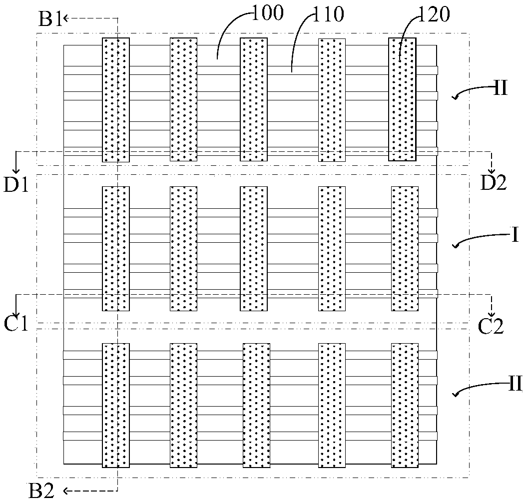
[0024] Currently, a discrete metal layer is usually formed on the interlayer dielectric layer above the isolation structure as a metal resistor device (Metal Resistor Device). When forming the interlayer dielectric layer, since the region corresponding to the isolation structure is a sparse area (Iso Area), after the planarization process for forming the interlayer dielectric layer, the top of the interlayer dielectric layer is flat The accuracy is poor, and the top of the interlayer dielectric layer is prone to a dishing problem, which leads to a decrease in the performance of the semiconductor structure.

[0025] In order to solve the technical problem, the present invention forms discrete dummy gates on the substrates of the...


PUM


Abstract

Disclosed are a semiconductor structure and a forming method thereof. The forming method comprises the following steps that a substrate is provided, wherein the substrate comprises a high-resistance device area, and the high-resistance device area is composed of a device area and an edge area; separated virtual pseudo gates are formed on the substrate of the device area and the edge area; and an interlayer dielectric film is formed on the substrate exposed out of the virtual pseudo gates, wherein the interlayer dielectric film covers the tops of the virtual pseudo gates; the interlayer dielectric film is subjected to planarization treatment, so that the residual interlayer dielectric film exposes the tops of the virtual pseudo gates, and the residual interlayer dielectric film serves as aninterlayer dielectric layer. Compared with the scheme that the virtual pseudo gate is not formed, the method has the advantage that in the planarization process in the subsequent formation of the interlayer dielectric layer, the top flatness of the interlayer dielectric layer can be improved, and the problem of top dishing of the interlayer dielectric layer can be improved, so that the performance of the semiconductor structure can be improved.

Description

technical field [0001] The invention relates to the field of semiconductor manufacturing, in particular to a semiconductor structure and a forming method thereof. Background technique [0002] In semiconductor manufacturing, with the development trend of VLSI, the feature size of integrated circuits continues to decrease. In order to adapt to the reduction of feature size, the channel length of MOSFET devices is also continuously shortened. However, as the channel length of the device is shortened, the distance between the source and the drain of the device is also shortened, so the control ability of the gate to the channel becomes worse, and the gate voltage pinches off the channel. The difficulty is also increasing, making the phenomenon of subthreshold leakage (subthreshold leakage), the so-called short-channel effect (SCE: short-channel effects) more likely to occur. [0003] Therefore, in order to better adapt to the reduction of feature size, the semiconductor proce...

Claims


Application Information

Patent Timeline
Patent Type & Authority Applications(China)
IPC IPC(8): H01L27/06H01L21/8234
CPCH01L21/823431H01L21/823481H01L27/0629
Inventor 周飞
Owner SEMICONDUCTOR MANUFACTURING INTERNATIONAL (BEIJING) CORP
Why Eureka
Try Eureka