Image sensor, method of manufacturing the same, identification device and apparatus thereof

A technology of image sensor and manufacturing method, which is applied in the fields of identification devices and equipment, image sensors and their manufacturing, can solve problems affecting imaging quality, etc., and achieve the effect of improving the quantum effect

Pending Publication Date: 2018-12-11
SHENZHEN FUSHI TECH CO LTD
View PDF0 Cites 1 Cited by
  • Summary
  • Abstract
  • Description
  • Claims
  • Application Information

AI Technical Summary

Problems solved by technology

However, when infrared or near-infrared light with a longer wavelength needs to be imaged, it often bypasses the photodiode due to its strong penetrating ability and cannot be fully absorbed and converted into an electrical signal, resulting in The quantum efficiency (Quantum Efficiency, QE) of traditional image sensors is low when imaging infrared or near-infrared light, which affects the imaging quality

Method used


Image

  • Image sensor, method of manufacturing the same, identification device and apparatus thereof
  • Image sensor, method of manufacturing the same, identification device and apparatus thereof
  • Image sensor, method of manufacturing the same, identification device and apparatus thereof

Examples


Embodiment Construction

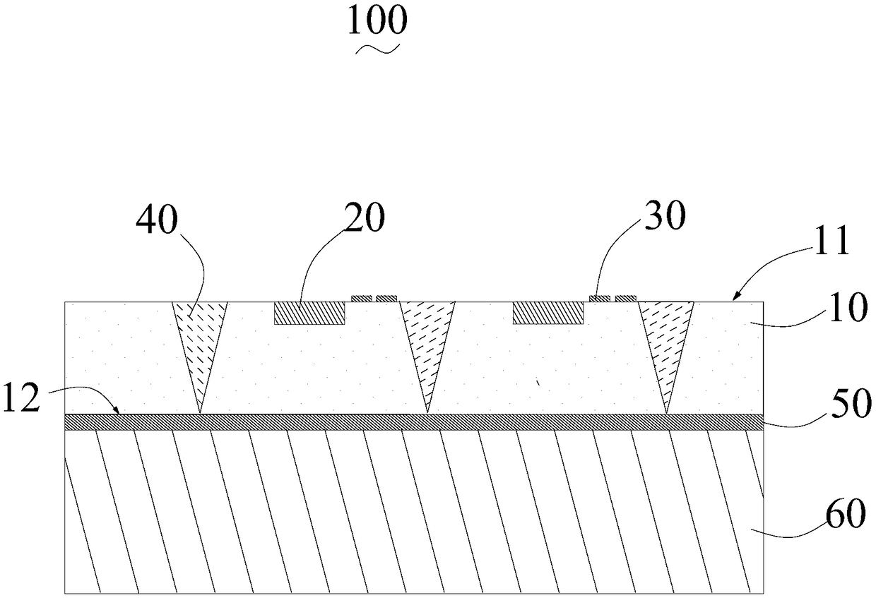
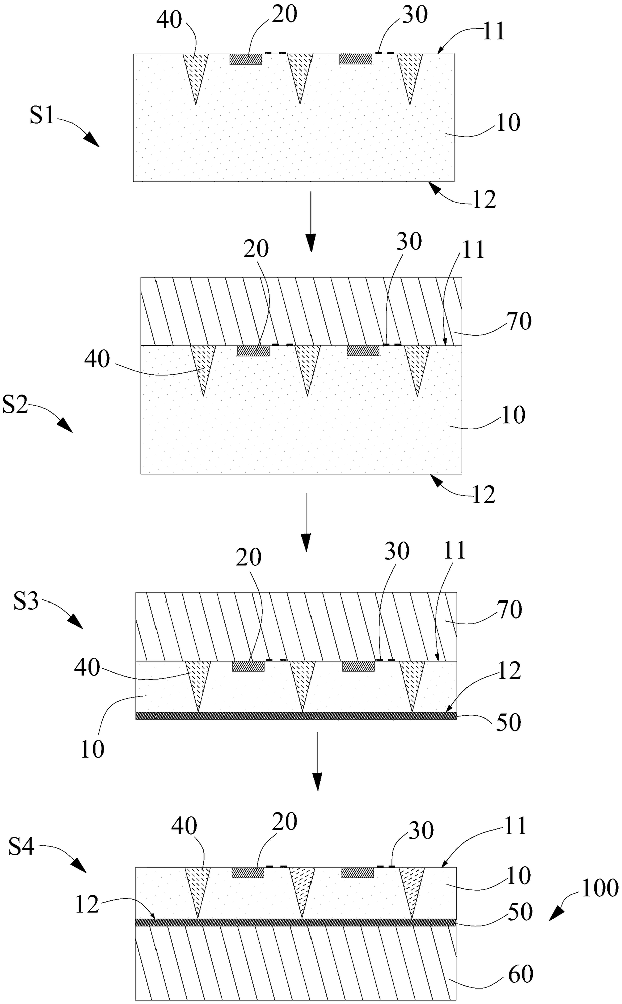
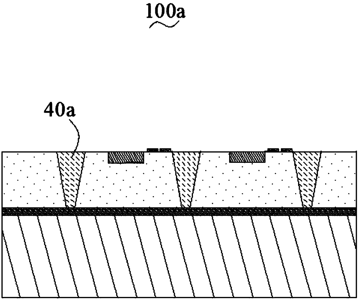
[0038] In order to make the purpose, technical solution and advantages of the present application clearer, the present application will be further described in detail below in conjunction with the accompanying drawings and implementation methods. It should be understood that the specific implementation manners described here are only used to explain the present application, and are not intended to limit the present application.

[0039] The following disclosure provides many different implementations or examples for implementing different structures of the present application. In order to simplify the disclosure of the present application, components and settings of specific examples are described below. Of course, they are examples only and are not intended to limit the application. Furthermore, the present application may repeat reference numerals and / or reference letters in various instances, such repetition is for the purpose of simplicity and clarity and does not in itse...


PUM


Abstract

The present application is applicable to the field of photoelectric technology, and provides an image sensor including a semiconductor substrate, a photodiode, and a reflective layer. The semiconductor substrate includes an upper surface and a lower surface arranged opposite to each other. The photodiode is formed inside the semiconductor substrate on one side of the upper surface. The photodiodereceives imaging light reflected by a target and converts the received imaging light into an electrical signal. The reflective layer is disposed on a propagation path of the imaging light passing through the photodiode for reflecting the imaging light passing through the photodiode without being converted into an electrical signal back to the photodiode. The present application also provides a method for manufacturing an image sensor, an identification device and apparatus.

Description

technical field [0001] The present application belongs to the field of optoelectronic technology, and in particular relates to an image sensor, a manufacturing method thereof, an identification device and equipment. Background technique [0002] The structure of traditional image sensors is mainly used to image visible light. Because the wavelength of visible light is relatively short, the penetration depth of photodiodes is relatively shallow, and most of them can be absorbed by photodiodes and converted into electrical signals. However, when infrared or near-infrared light with a longer wavelength needs to be imaged, it often bypasses the photodiode due to its strong penetrating ability and cannot be fully absorbed and converted into an electrical signal, resulting in Traditional image sensors have low quantum efficiency (Quantum Efficiency, QE) when imaging infrared or near-infrared light, which affects imaging quality. Contents of the invention [0003] The technical ...

Claims


Application Information

Patent Timeline
Patent Type & Authority Applications(China)
IPC IPC(8): H01L27/146
CPCH01L27/1462H01L27/14643H01L27/14685
Inventor 王小明
Owner SHENZHEN FUSHI TECH CO LTD
Why Eureka
Try Eureka