Method for magnesia nanometer line epitaxial growth from strontium titanate monocrystal chip

A technology of strontium titanate substrate and nano-film, which is applied in the field of microelectronic materials, can solve problems such as difficulty in structural control, and achieve the effect of enhancing quantum effects

Inactive Publication Date: 2007-07-25
UNIV OF ELECTRONICS SCI & TECH OF CHINA
View PDF0 Cites 0 Cited by
  • Summary
  • Abstract
  • Description
  • Claims
  • Application Information

AI Technical Summary

Problems solved by technology

This requirement makes structural control more difficult relative to the limitations of growing zero-dimensional and two-dimensional structures

Method used


Image

  • Method for magnesia nanometer line epitaxial growth from strontium titanate monocrystal chip
  • Method for magnesia nanometer line epitaxial growth from strontium titanate monocrystal chip
  • Method for magnesia nanometer line epitaxial growth from strontium titanate monocrystal chip

Examples


Embodiment Construction

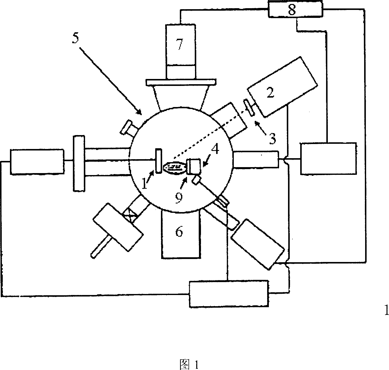
[0022] The magnesium oxide nano film with ordered surface periodic structure prepared by the present invention is to use laser molecular beam epitaxy (L-MBE) to ablate and peel off the magnesium oxide ceramic target material on the strontium titanate (001) single crystal substrate , prepared under high vacuum conditions.

[0023] The structure diagram of the laser molecular beam epitaxy system (L-MBE) used to prepare magnesium oxide nano-films with ordered surface periodic structure according to the present invention is shown in FIG. 1 .

[0024] Specifically, the steps of the preparation method of the present invention are:

[0025] (1) Selection of magnesia ceramic target: high-purity magnesia polycrystalline ceramic target (above 99.9%), Φ50mm×5mm;

[0026] (2) Selection of substrate material: select a single crystal strontium titanate (001) substrate, and place the substrate on the substrate box 9;

[0027] (3) Place the magnesia ceramic target on the target platform 1, ...


PUM

PropertyMeasurementUnit
diameteraaaaaaaaaa
thicknessaaaaaaaaaa
wavelengthaaaaaaaaaa

Abstract

The method to epitaxial grow magnesia nano line on single crystal substrate of strontium titanate relates to micro-electronics material field particular to the application on hetero epitaxy center nano line and its periodic surface structure of oxide (magnesis)-composite oxide (strontium titanate). Wherein, on vacuum condition, taking thermal treatment to the said substrate to strip with laser the magnesia ceramics material and depositing the laser plasma on the substrate to obtain magnesia thin membrane; monitoring the depositing process till forming said nano line. The product has special properties on optical, electric, magnetism, chemistry.

Description

technical field [0001] The invention relates to the field of microelectronic materials, in particular to a method applied to oxide (magnesium oxide)-composite oxide (strontium titanate) heterogeneous epitaxy to prepare a nano film with a surface periodic structure. Background technique [0002] Nanowires and nanobelts are a new type of quasi-one-dimensional structure materials, which have attracted extensive attention in research and application. This structure shows superior electrical, optical, mechanical, and thermal properties, and its application range covers chemical biosensors, field-effect transistors, functional ceramics, optoelectronic devices, and logic integrated circuits. [0003] Based on a deep understanding of material properties, the rational design and control of this one-dimensional structure creates conditions for the further preparation of new nanostructured materials and devices. Typically, growing one-dimensional structures requires controlling two di...

Claims


Application Information

Patent Timeline
Patent Type & Authority Patents(China)
IPC IPC(8): C01F5/02B82B3/00
Inventor 梁柱李言荣朱俊张鹰
Owner UNIV OF ELECTRONICS SCI & TECH OF CHINA
Why Eureka
Try Eureka