Pixel arrangement structure and display device
A pixel arrangement and pixel technology, applied in electrical components, electric solid state devices, circuits, etc., can solve the problem of low resolution of display devices
- Summary
- Abstract
- Description
- Claims
- Application Information
AI Technical Summary
Problems solved by technology
Method used
Image

Examples
Embodiment Construction
[0025] The following descriptions of the various embodiments refer to the accompanying drawings to illustrate specific embodiments that the present application can be used to implement. The directional terms mentioned in this application, such as [top], [bottom], [front], [back], [left], [right], [inside], [outside], [side], etc., are for reference only The orientation of the attached schema. Therefore, the directional terms used are used to illustrate and understand the application, but not to limit the application. In the figures, structurally similar elements are denoted by the same reference numerals.
[0026] The present application provides a pixel arrangement structure and a display device. The existing display device has a problem of low resolution, and this embodiment can improve this defect.
[0027] The application will be further described below in conjunction with the accompanying drawings and specific embodiments:
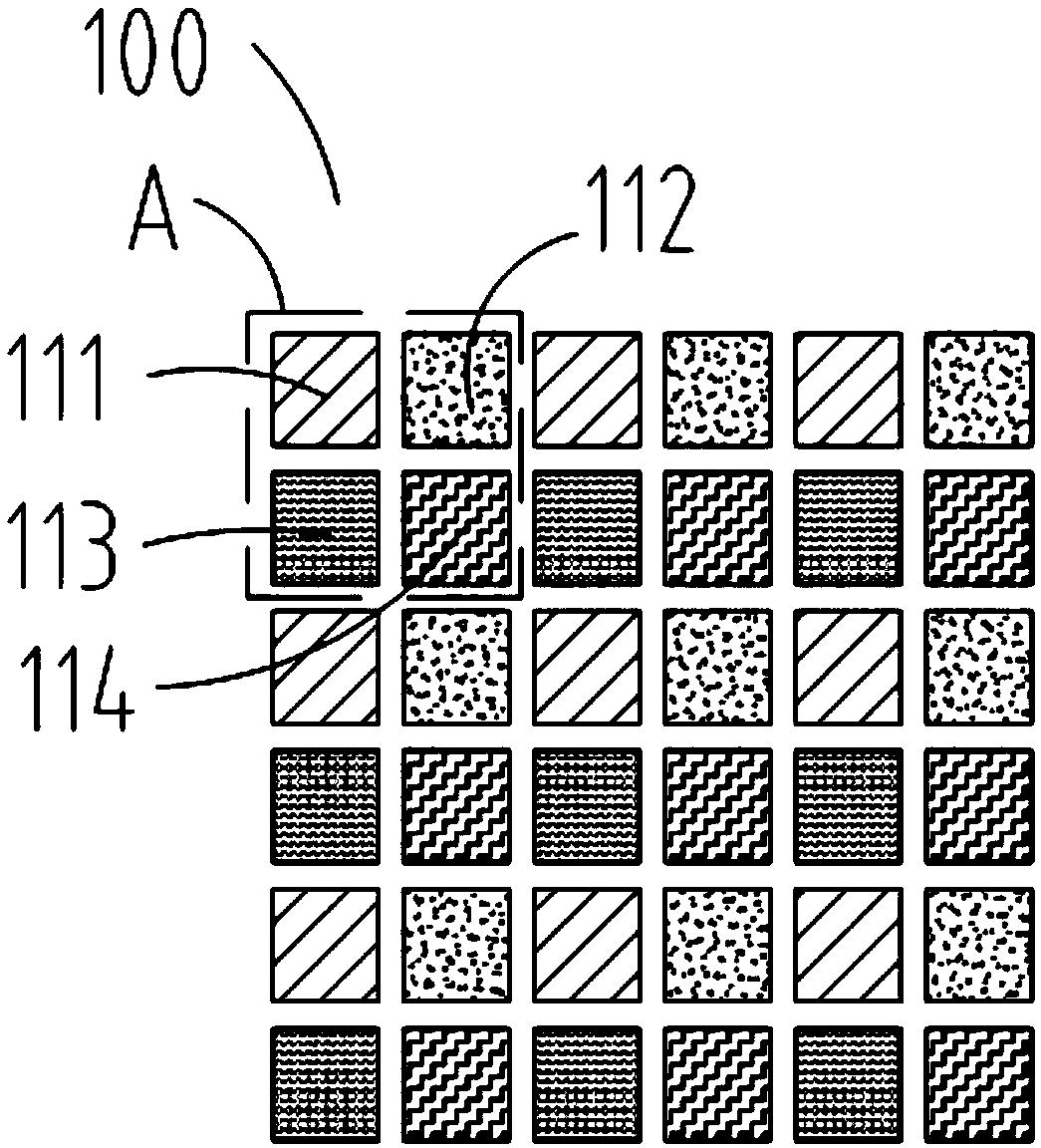
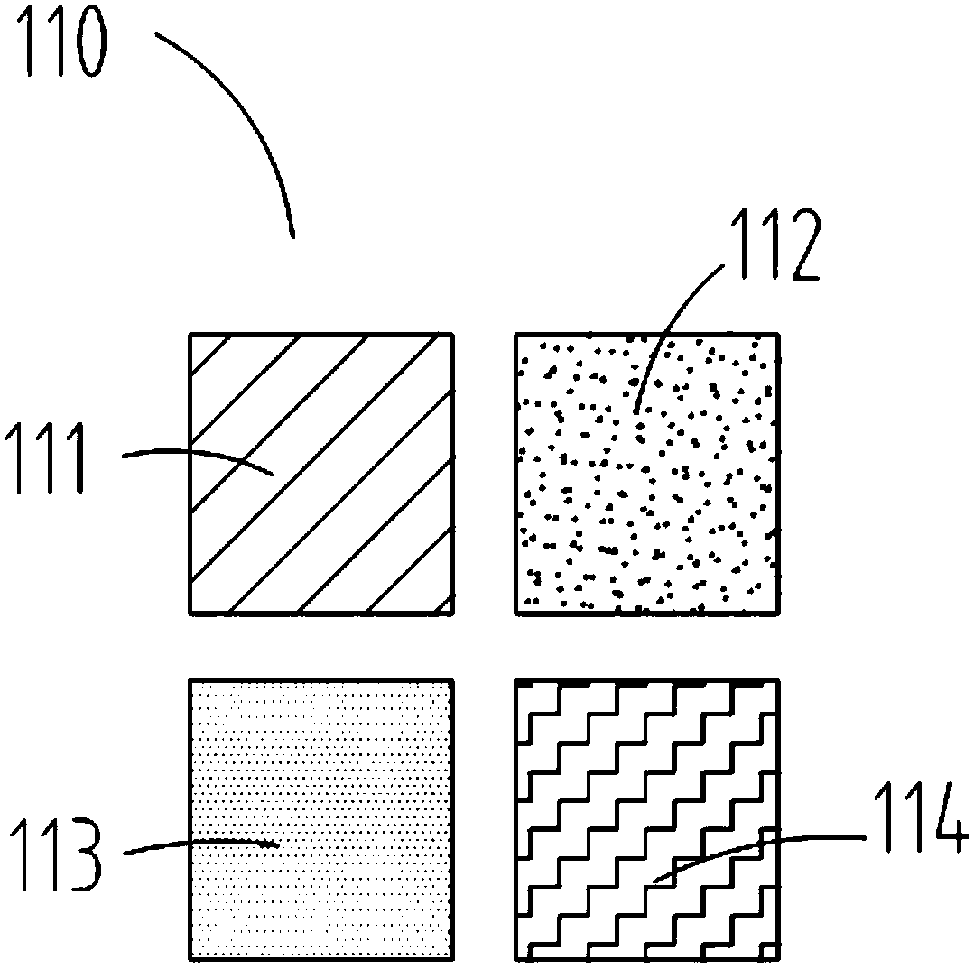
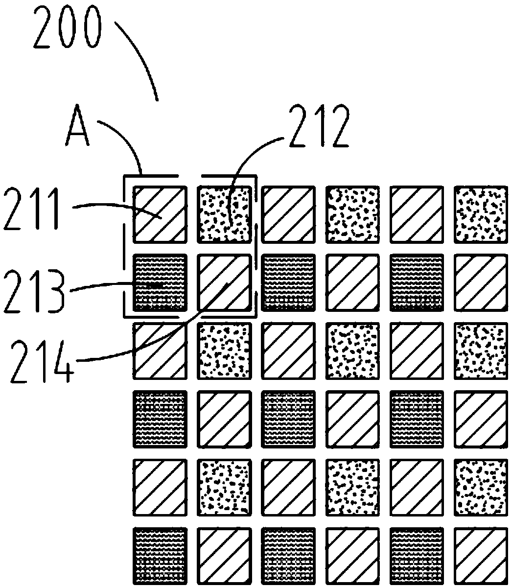
[0028] see figure 1 , figure 1 A schematic...
PUM
 Abstract
Description
Claims
Application Information
 - R&D
- Intellectual Property
- Life Sciences
- Materials
- Tech Scout
- Unparalleled Data Quality
- Higher Quality Content
- 60% Fewer Hallucinations
Browse by: Latest US Patents, China's latest patents, Technical Efficacy Thesaurus, Application Domain, Technology Topic, Popular Technical Reports.
© 2025 PatSnap. All rights reserved.Legal|Privacy policy|Modern Slavery Act Transparency Statement|Sitemap|About US| Contact US: help@patsnap.com