Supercharge Your Innovation With Domain-Expert AI Agents!

Pixel arrangement structure and display device

a technology of pixel arrangement and display device, which is applied in the field of display technologies, can solve the problems of high quality and high resolution of oled display panel production, and still faces many challenges, and achieve the effect of improving the sensory resolution of the display device and higher the sensory resolution

Active Publication Date: 2021-03-02
WUHAN CHINA STAR OPTOELECTRONICS SEMICON DISPLAY TECH CO LTD
View PDF23 Cites 0 Cited by
  • Summary
  • Abstract
  • Description
  • Claims
  • Application Information

AI Technical Summary

Benefits of technology

This approach enhances sensory resolution and reduces the risk of wrinkling during FMM opening, simplifying the display device structure and reducing production costs while maintaining high-resolution performance.

Problems solved by technology

Currently, mainstream pixel arrangement structures use a red / green / blue (RGB) stripe configuration and a pentile (P) arrangement; however, production of OLED display panels, having high quality and high resolution, still faces many challenges.

Method used


Image

  • Pixel arrangement structure and display device
  • Pixel arrangement structure and display device
  • Pixel arrangement structure and display device

Examples


Embodiment Construction

[0034]The embodiments described herein with reference to the accompanying drawings are explanatory, illustrative, and used to generally understand the present disclosure. Furthermore, directional terms described by the present disclosure, such as top, bottom, front, back, left, right, inner, outer, side, etc., are only directions by referring to the accompanying drawings, and thus the used terms are used only for the purpose of describing embodiments of the present disclosure and are not intended to be limiting of the present disclosure. In the drawings, modules with similar structures are labeled with the same reference number.

[0035]The present disclosure provides a pixel arrangement structure and a display device to address technical problems of low resolution of conventional display devices and solves the drawbacks.

[0036]The present disclosure will be further described below in conjunction with accompanying drawings and specific embodiments.

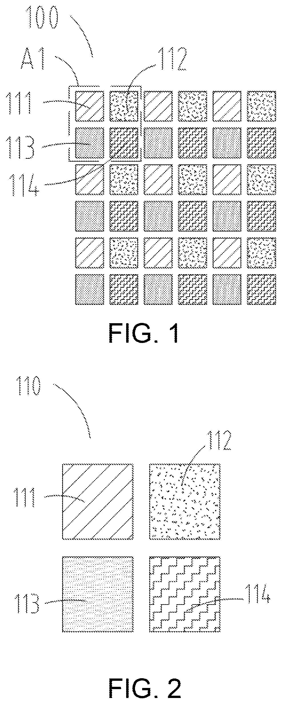
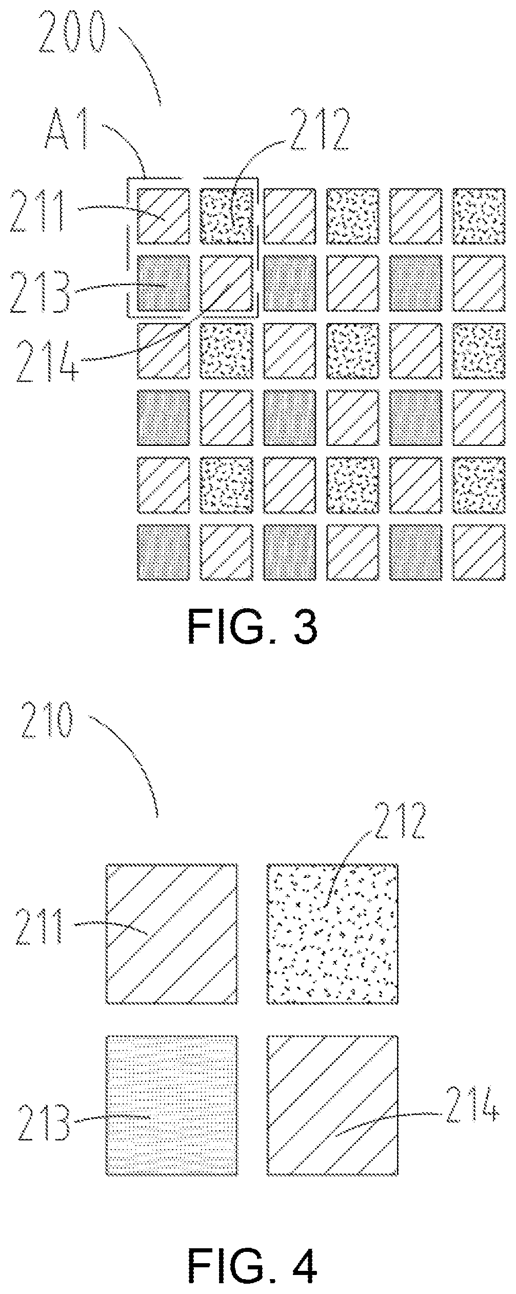
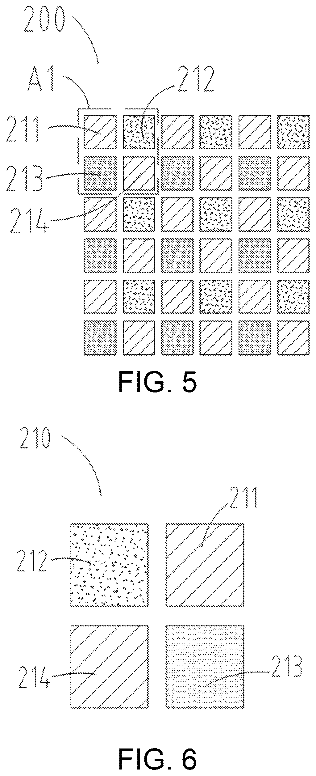
[0037]Refer to FIG. 1, a schematic stru...


PUM


Abstract

A pixel arrangement structure and a display device are provided. The pixel arrangement structure includes a plurality of repeating units. The repeating units include a first sub-pixel, a second sub-pixel, a third sub-pixel, and a fourth sub-pixel. Center points of the first sub-pixel, the second sub-pixel, the third sub-pixel, and the fourth sub-pixel in a same repeating unit form a quadrilateral. Four adjacent sub-pixels in adjacent repeating units constitute a shared pixel, and the shared pixel includes at most two sub-pixels belonging to the same repeating unit.

Description

FIELD OF INVENTION[0001]The present disclosure relates to the field of display technologies, and more particularly to a pixel arrangement structure and a display device.BACKGROUND OF INVENTION[0002]In flat panel display technologies, organic light emitting diode (OLED) display devices have many advantages of light weight, active illumination, fast response times, wide viewing angles, wide color gamut, high brightness, low power consumption, etc. The OLED display devices have gradually become third generation display technology after liquid crystal display devices. Currently, mainstream pixel arrangement structures use a red / green / blue (RGB) stripe configuration and a pentile (P) arrangement; however, production of OLED display panels, having high quality and high resolution, still faces many challenges.[0003]Therefore, there is a need for a pixel arrangement structure and a display device to solve the above problems.SUMMARY OF INVENTION[0004]The present disclosure provides a pixel a...

Claims


Application Information

Patent Timeline
Patent Type & Authority Patents(United States)
IPC IPC(8): H01L27/32
CPCH01L27/3216H01L27/3213H01L27/3218H01L27/3244H10K59/351H10K59/352H10K59/353H10K59/12
Inventor WANG, ZHENG
Owner WUHAN CHINA STAR OPTOELECTRONICS SEMICON DISPLAY TECH CO LTD
Features
  • R&D
  • Intellectual Property
  • Life Sciences
  • Materials
  • Tech Scout
  • Unparalleled Data Quality
  • Higher Quality Content
  • 60% Fewer Hallucinations
Learn More