

Array substrate and liquid crystal display panel
An array substrate and storage capacitor technology, applied in nonlinear optics, instruments, optics, etc., can solve the problems of low product yield, easy correction of broken wires, broken data lines 200, etc., to improve product yield, metal The effect of reducing the shading area and increasing the aperture ratio
- Summary
- Abstract
- Description
- Claims
- Application Information
AI Technical Summary
Problems solved by technology
Method used
Image

Examples
Embodiment 1
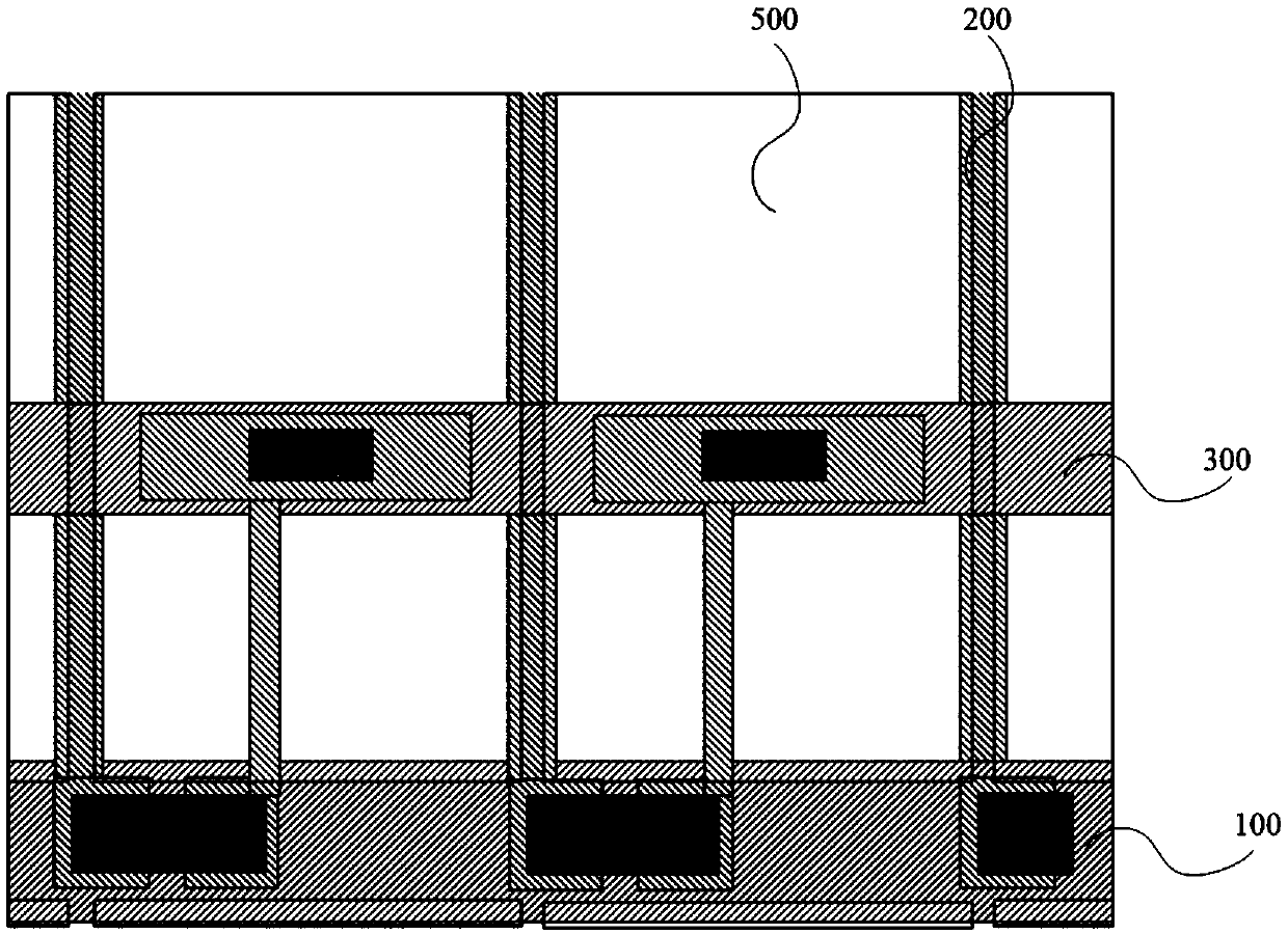
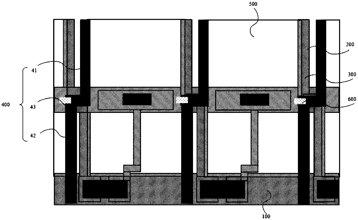
[0042] figure 2 For the circuit design diagram of the array substrate provided by the embodiment of the present invention, refer to figure 2 As shown, one aspect of the present invention provides an array substrate, including: scanning lines 100, data lines 200, storage capacitor bus lines 300, and storage capacitor branch lines 400; A pixel area 500 is formed between two adjacent scan lines 100 and two adjacent data lines 200; the storage capacitor bus 300 is arranged parallel to the scan line 100 and crosses the pixel area 500, and the storage capacitor bus 300 and the surrounding composite pixel area One of the scanning lines 100 of 500 is electrically connected; the storage capacitor branch line 400 extends along the direction of the data line 200 and is arranged close to the data line 200, the storage capacitor branch line 400 is electrically connected to the storage capacitor bus 300, and the storage capacitor branch line 400 is made of conductive Made of transparent ...
Embodiment 2
[0063] An embodiment of the present invention also provides a liquid crystal display panel, including: the array substrate as described in the above embodiment, a color filter substrate disposed opposite to the array substrate, and a color filter substrate sandwiched between the array substrate and the color filter substrate layer of liquid crystal molecules.
[0064] The general structure of a liquid crystal display panel includes a polarizer, a color filter substrate, a liquid crystal layer, an array substrate, and a polarizer arranged sequentially from top to bottom. Among them, the function of the polarizer is to control the light of the backlight to only let the light in a specific direction pass through, and filter out the light in other directions. The light processed by the polarizing plate can control the brightness of the light exiting the display screen through the twisting action of the liquid crystal molecules, thereby controlling the brightness of the light exiti...
PUM
 Abstract
Description
Claims
Application Information