
Metal-insulator-semiconductor-insulator-metal (MISIM) device, method of operation, and memory device including the same

A technology of semiconductors and insulators, which is applied in the direction of semiconductor devices, electric solid-state devices, bulk negative resistance effect devices, etc., and can solve problems such as incompatibility of complementary metal oxide semiconductors

Inactive Publication Date: 2019-04-05
TAIWAN SEMICON MFG CO LTD +1
View PDF0 Cites 0 Cited by
  • Summary
  • Abstract
  • Description
  • Claims
  • Application Information

AI Technical Summary

Problems solved by technology

On the other hand, for the three-terminal configuration, existing negative differential resistance devices are CMOS incompatible, or can only operate in single negative differential resistance mode

Method used


Image

  • Metal-insulator-semiconductor-insulator-metal (MISIM) device, method of operation, and memory device including the same
  • Metal-insulator-semiconductor-insulator-metal (MISIM) device, method of operation, and memory device including the same
  • Metal-insulator-semiconductor-insulator-metal (MISIM) device, method of operation, and memory device including the same

Examples


Embodiment Construction

[0142] The present disclosure provides many different embodiments, or examples, for implementing the different features of the disclosure. The following disclosure describes specific examples of various components and their arrangements to simplify the description. Of course, these specific examples are not intended to be limiting. For example, if the present disclosure describes that a first feature is formed on or above a second feature, it means that it may include embodiments in which the above-mentioned first feature is in direct contact with the above-mentioned second feature, and may also include Embodiments in which an additional feature is formed between the first feature and the second feature such that the first feature and the second feature may not be in direct contact. In addition, the same reference signs and / or symbols may be reused in different examples in the following publications. These repetitions are for simplicity and clarity and are not intended to li...


PUM


Abstract

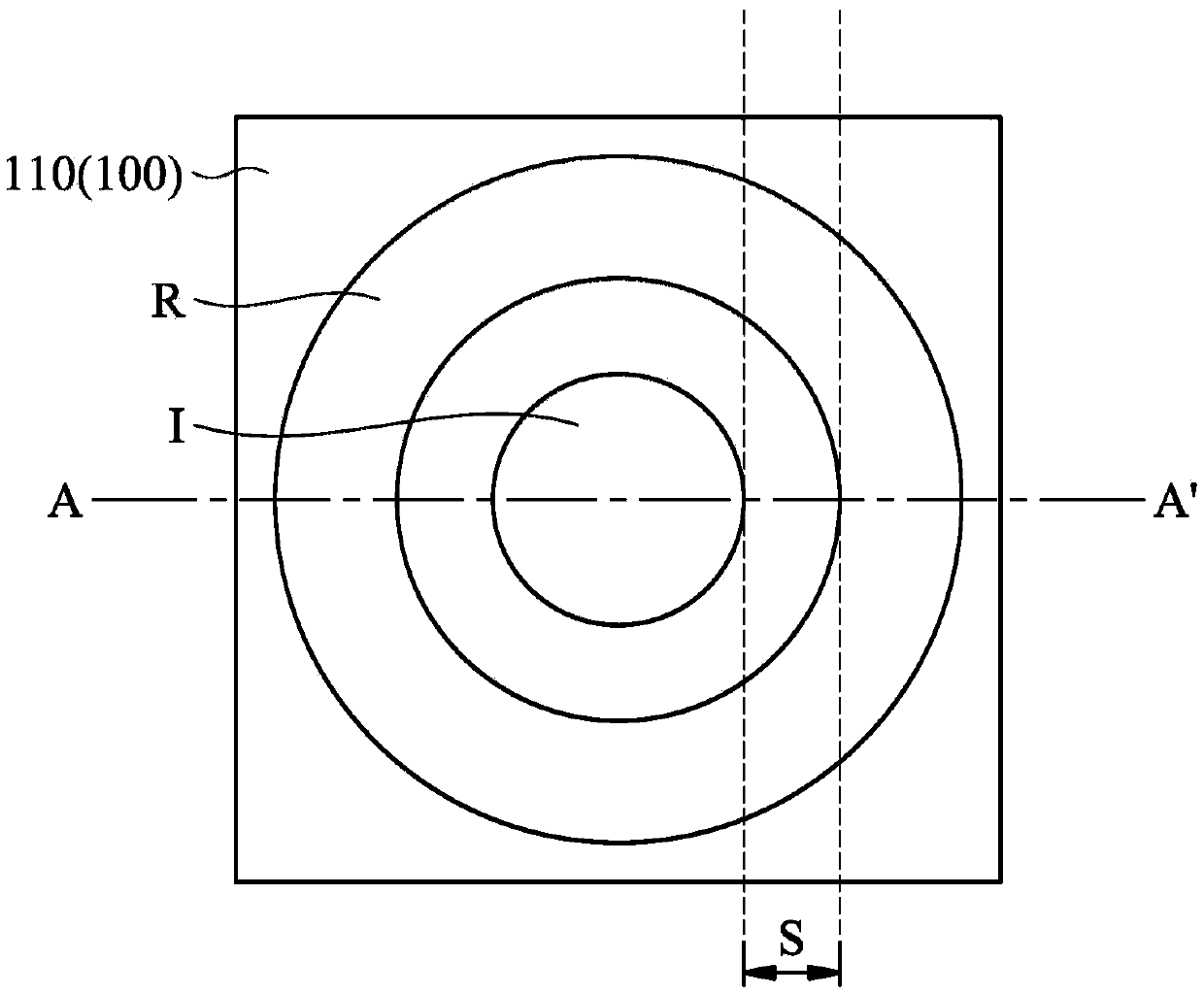
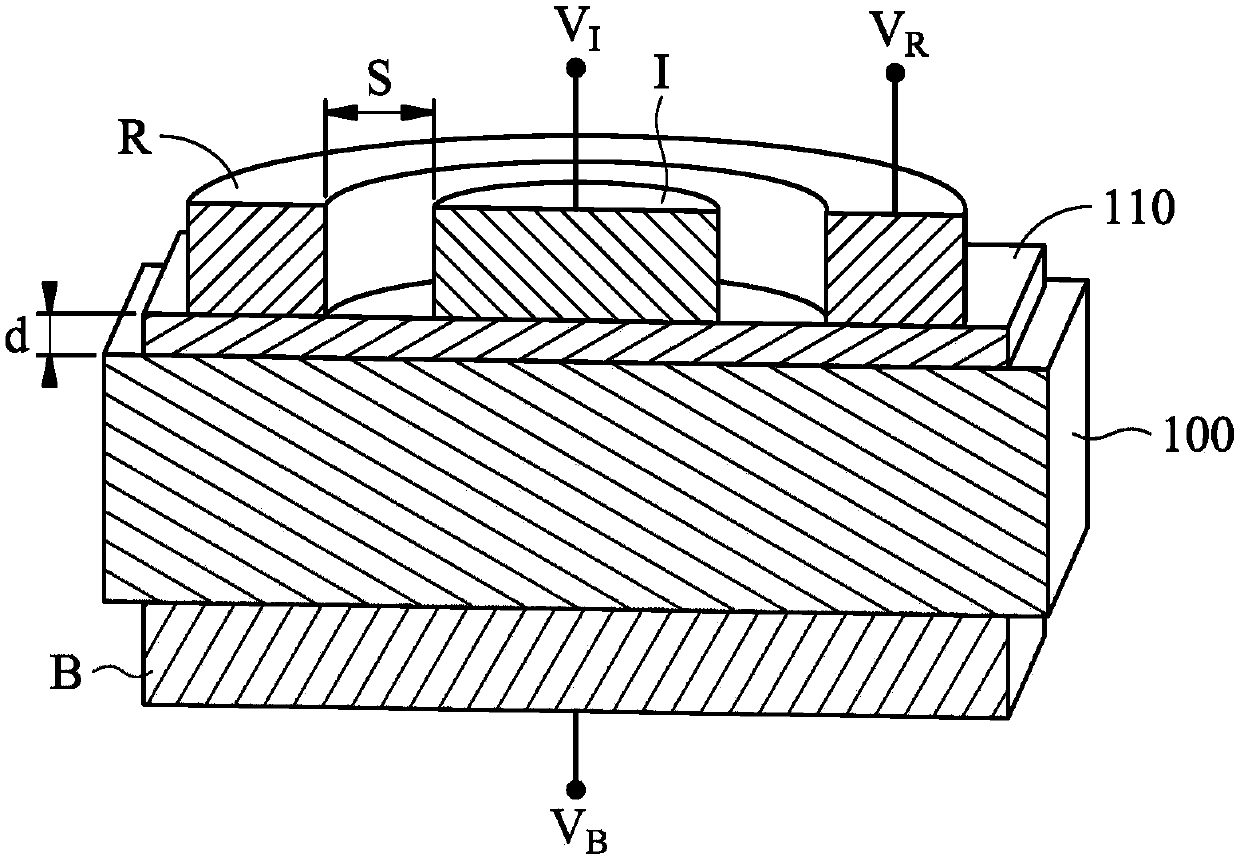
A metal-insulator-semiconductor-insulator-metal (MISIM) device includes a semiconductor layer, an insulating layer disposed over an upper surface of the semiconductor layer, a back electrode disposedover a lower surface of the semiconductor layer opposing the upper surface, and first and second electrodes disposed over the insulating layer and spaced-apart from each other.

Description

technical field [0001] The present disclosure relates to a metal-insulator-semiconductor-insulator-metal (MISIM) device, particularly a MISIM device that can operate in a single negative differential resistance (NDR) mode or a dual NDR mode. Background technique [0002] Negative differential resistance (NDR) devices are available in two-terminal or three-terminal configurations. For two-terminal configurations, adjustment of the negative differential resistance device is difficult to allow operation of the negative differential resistance device over an extended operating range. On the other hand, for the three-terminal configuration, existing negative differential resistance devices are CMOS incompatible, or can only operate in a single negative differential resistance mode. Contents of the invention [0003] The present disclosure provides a metal-insulator-semiconductor-insulator-metal (MISIM) device, comprising: a semiconductor layer; an insulating layer disposed on ...

Claims


Application Information

Patent Timeline
IPC IPC(8): H01L47/00
CPCH10N80/00G11C11/56G11C13/0007G11C11/34H01L29/88H01L29/417H10B99/00H10N89/02H10N80/10
Inventor 胡振国杨昶丰林浩雄潘正圣
Owner TAIWAN SEMICON MFG CO LTD
Learn More