a display device

A technology for display devices and display areas, which is applied in identification devices, nonlinear optics, instruments, etc., and can solve problems such as large resistance, damage to lines caused by static electricity, and decline in anti-static capabilities

Active Publication Date: 2022-02-01
AU OPTRONICS KUNSHAN CO LTD
View PDF33 Cites 0 Cited by
  • Summary
  • Abstract
  • Description
  • Claims
  • Application Information

AI Technical Summary

Problems solved by technology

[0002] With the development of display device technology, the definition of display devices is getting higher and higher, making the thin film transistor lattice metal lines of display devices thinner and denser, and the available area of ​​circuit design is getting smaller and smaller, so It is necessary to simplify some electrostatic protection (ESD) protection circuits, resulting in a decrease in the antistatic ability of the thin film transistor lattice
When static electricity accumulates on the surface of the substrate, it is not easy to dissipate. When the static electricity is released, it is easy to cause static electricity to damage the circuit and cause damage.
[0003] At present, due to the touch function requirements of iTP products, the high-impedance electrostatic film on the side of the color-resistive layer has a strict resistance limit, which is required to be 5×10 8 ~9×10 9 Between ohms, a large resistance value is likely to cause static electricity accumulation
[0004] In addition, due to the decline of anti-static ability, many manual processing processes and lamination processes will also generate high static electricity during the post-plywood process, causing static electricity to damage the circuit

Method used


Image

  • a display device
  • a display device
  • a display device

Examples


no. 1 example

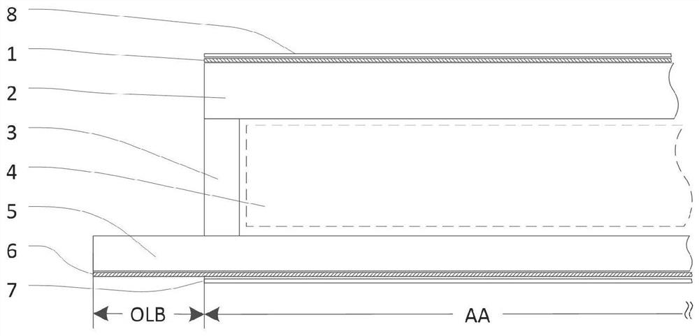
[0046] figure 1 It is a partial cross-sectional structural schematic diagram of a display device according to the first embodiment of the present invention. Such asfigure 1 As shown, in the first embodiment of the present invention, a display device is proposed, including: a first substrate 5, a second substrate 2, a display molecular layer 4, a first polarizer 7 and a second polarizer 8, wherein the first The substrate 5 includes an adjacent display area AA and a bonding area OLB. In this embodiment, the first substrate 5 is an active array substrate, the second substrate 2 is a color filter substrate, the first substrate 5 is opposite to the second substrate 2, and the position of the second substrate 2 corresponds to that of the first substrate 5 The display area AA. The first polarizer 7 is arranged on the outer surface of the first substrate 5 (the side of the first substrate 5 facing away from the second substrate 2), and the second polarizer 8 is arranged on the outer...


PUM

PropertyMeasurementUnit
impedanceaaaaaaaaaa

Abstract

A display device, comprising: a first substrate, including an opposite first inner surface and a first outer surface, an adjacent display area, a bonding area, and a plurality of thin film transistors, and the thin film transistors are arranged on the inner surface, And the position corresponds to the display area; the second substrate is arranged opposite to the display area, including a second inner surface and a second outer surface opposite, a first color resistance and a second color resistance, and the first color resistance and the second color resistance The second color resistance is respectively arranged on the second inner surface; the display molecule layer is arranged between the first substrate and the second substrate; the display device also includes: an electrical shielding layer arranged on the first substrate The first outer surface; wherein, the electrical shielding layer includes a first shielding area and a second shielding area, the first shielding area is arranged at a position corresponding to the first color resistance, and the second shielding area is located at a position corresponding to the bonding area.

Description

technical field [0001] The invention relates to a display device, in particular to a display device with an electrostatic protection structure. Background technique [0002] With the development of display device technology, the definition of display devices is getting higher and higher, making the thin film transistor lattice metal lines of display devices thinner and denser, and the available area of ​​circuit design is getting smaller and smaller, so It is necessary to simplify some electrostatic protection (ESD) protection circuits, resulting in a decline in the antistatic ability of the thin film transistor lattice. When static electricity accumulates on the surface of the substrate, it is not easy to dissipate. When the static electricity is released, it is easy to cause static electricity to damage the circuit and cause damage. [0003] At present, due to the touch function requirements of iTP products, the high-impedance electrostatic film on the side of the color-r...

Claims


Application Information

Patent Timeline
Patent Type & Authority Patents(China)
IPC IPC(8): G09F9/00G02F1/1333
Inventor 朱永铨郑朝雲陈珊芳刘海燕
Owner AU OPTRONICS KUNSHAN CO LTD
Why Eureka
Try Eureka