Semiconductor package substrate increasing static dissipation capability

A technology for packaging substrates and static dissipation, which is applied in semiconductor devices, semiconductor/solid-state device components, electric solid-state devices, etc., and can solve the problems of general products without structure, changing design structure, and inconvenience.

Inactive Publication Date: 2008-07-23
CHIPMOS TECH INC
View PDF0 Cites 5 Cited by
  • Summary
  • Abstract
  • Description
  • Claims
  • Application Information

AI Technical Summary

Problems solved by technology

Therefore, this "embedded capacitor" structure is quite special, and at the same time changes the design structure of the chip and substrate in the packaged product, and the "embedded capacitor" structure is hidden between the chip and the substrate, that is, the electrostatic charge is accumulated on the In the shielding gap that cannot be eliminated, there is no obvious benefit for static electricity dissipation during the packaging process
[0006] It can be seen that the above-mentioned existing semiconductor packaging substrate obviously still has inconvenience and defects in structure and use, and needs to be further improved urgently.
In order to solve the above-mentioned problems, the relevant manufacturers have tried their best to find a solution, but no suitable design has been developed for a long time, and the general products do not have a suitable structure to solve the above-mentioned problems. This is obviously related. The problem that the industry is eager to solve

Method used


Image

  • Semiconductor package substrate increasing static dissipation capability
  • Semiconductor package substrate increasing static dissipation capability
  • Semiconductor package substrate increasing static dissipation capability

Examples


no. 1 Embodiment

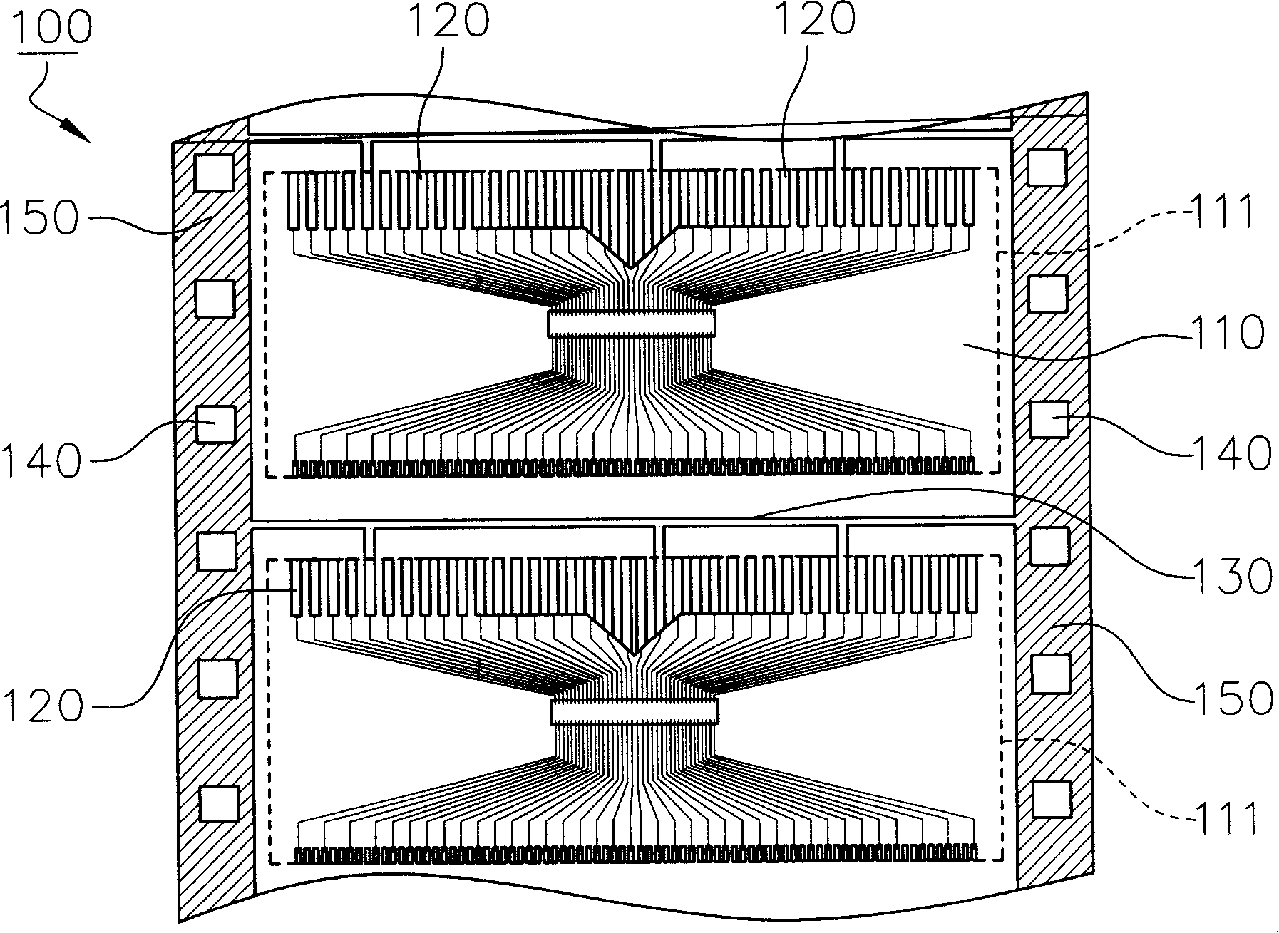
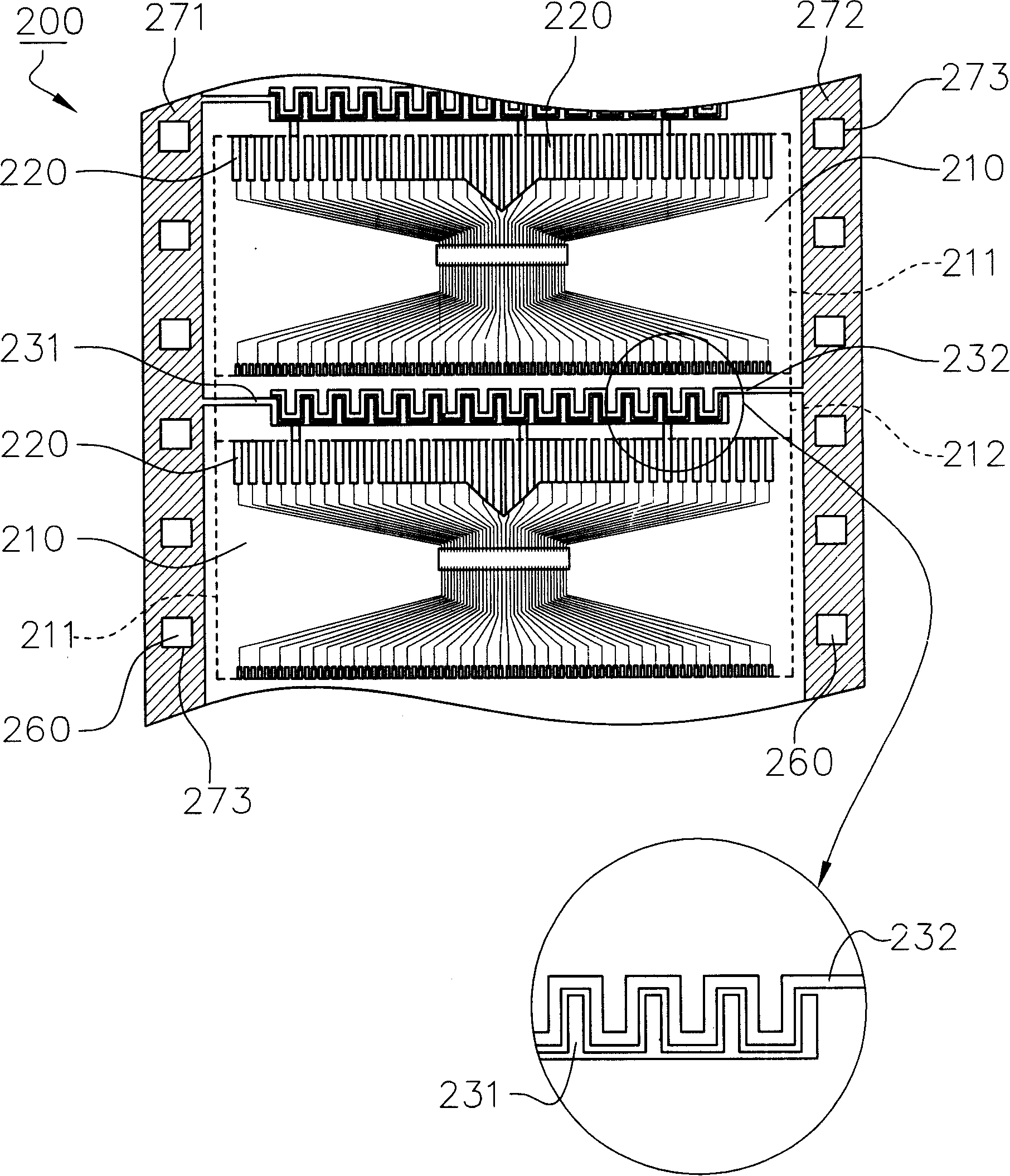
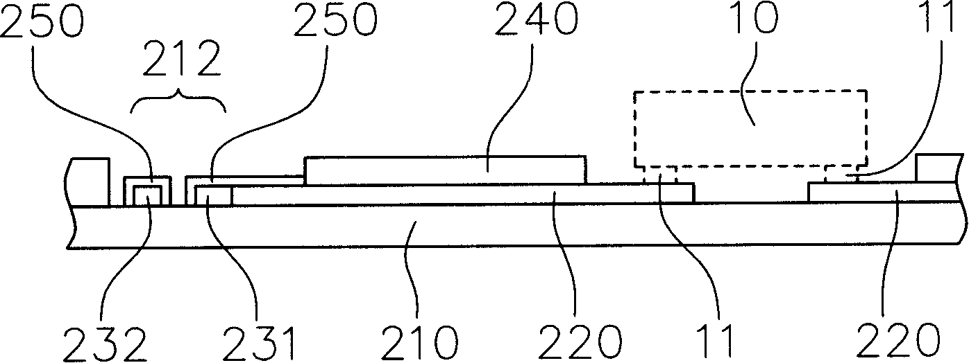
[0059] According to a first embodiment of the present invention, a semiconductor package substrate is disclosed. Such as figure 2 and image 3 As shown, the semiconductor package substrate 200 mainly includes a dielectric layer 210 , a plurality of pins 220 , a plurality of first electrostatic guiding lines 231 , a plurality of second electrostatic guiding lines 232 and a solder resist layer 240 . A surface of the dielectric layer 210 defines a plurality of packaging units 211 and a plurality of static dissipative regions 212 . After the packaging process, a semiconductor package structure can be cut out along the periphery of the package units 211 . Generally, these encapsulation units 211 can also be referred to as use areas. The static dissipative area 212 is located between or on the side of the packaging unit 211, and is used to disperse the static charge of the grounding pin or the pin with weak static resistance in these static dissipative areas 212 exposed outside ...


PUM


Abstract

The invention relates to a semiconductor package substrate capable of reinforcing static dissipating ability, comprising a dielectric layer, a plurality of pins, a plurality of first static guide circuits, a plurality of second guide circuits and a solder mask. The first static guide circuits and the second static circuits are formed in a plurality of static dissipating areas of the dielectric layer, the static dissipating areas are in electric insulating neighbored arrangement and are exposed out of the solder mast, further the first static guide circuits are connected with a part of pins, thereby reinforcing the static dissipating ability of the substrate in manufacture procedure.

Description

technical field [0001] The invention relates to a semiconductor packaging substrate, in particular to a semiconductor packaging substrate with enhanced electrostatic dissipation capability. Background technique [0002] Objects or human bodies will accumulate static electricity due to friction during the moving process. The electrostatic voltage is quite high, up to thousands of volts or even tens of thousands of volts. When it is discharged instantaneously, it will seriously damage the surrounding electronic components, that is, "electric discharge". In the process of semiconductor packaging, the problem of electrostatic discharge damage to integrated circuit chips will also be encountered. [0003] Such as figure 1 As shown, a conventional semiconductor package substrate 100 mainly includes a dielectric layer 110 , a plurality of pins 120 and a solder resist layer (not shown). A plurality of packaging units 111 are defined on the dielectric layer 110 . The pins 120 are ...

Claims


Application Information

Patent Timeline
Patent Type & Authority Applications(China)
IPC IPC(8): H01L23/498H01L23/60
CPCH01L2224/16225
Inventor 陈崇龙李明勋
Owner CHIPMOS TECH INC
Why Eureka
Try Eureka