

Semiconductor device and method for manufacturing same
A semiconductor and main body technology, applied in semiconductor/solid-state device manufacturing, semiconductor devices, transistors, etc., can solve problems such as degradation of operating characteristics of semiconductor devices
- Summary
- Abstract
- Description
- Claims
- Application Information
AI Technical Summary
Problems solved by technology
Method used
Image

Examples
Embodiment Construction
[0022] Hereinafter, some embodiments will be described in detail with reference to the accompanying drawings to help clearly understand the inventive concept.
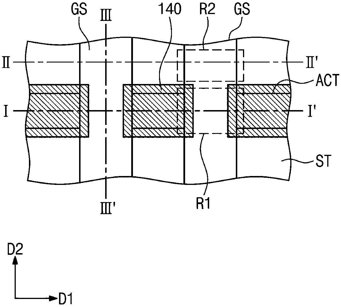
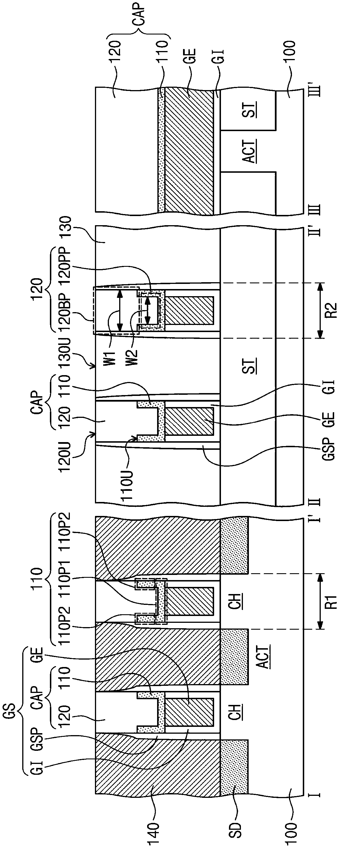
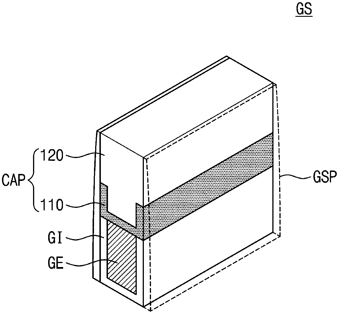
[0023] figure 1 A plan view illustrating a semiconductor device according to an exemplary embodiment is shown. figure 2 shows along the figure 1 Cross-sectional views taken along line II', line II-II' and line II-III' of . image 3 shows show figure 1 Perspective view of the gate structure.
[0024] refer to Figure 1 to Figure 3 , the substrate 100 may be provided thereon with a device isolation layer ST defining an active pattern ACT. The substrate 100 may be a silicon substrate, a germanium substrate, or a silicon-on-insulator (SOI) substrate, or may include a silicon substrate, a germanium substrate, or a silicon-on-insulator (SOI) substrate. The device isolation layer ST may include, for example, oxide, nitride or oxynitride. The active pattern ACT may extend in a direction D1 parallel to the top surface o...
PUM
 Abstract
Description
Claims
Application Information