Display screen device
A technology of display screen and display area, applied in identification devices, instruments, etc., can solve problems such as weak adsorption and 400 ink layer shedding, and achieve the effects of improving service life, avoiding ink shedding, and reducing maintenance costs.
- Summary
- Abstract
- Description
- Claims
- Application Information
AI Technical Summary
Problems solved by technology
Method used
Image

Examples
Embodiment Construction
[0028] The technical solutions in the embodiments of the present invention will be clearly and completely described below in conjunction with the accompanying drawings in the embodiments of the present invention. Obviously, the described embodiments are only part of the embodiments of the present invention, rather than the present invention. All examples in . Based on the embodiments of the present invention, all other embodiments obtained by persons of ordinary skill in the art without making creative efforts fall within the protection scope of the present invention.
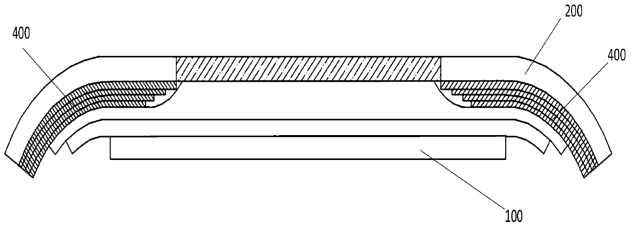
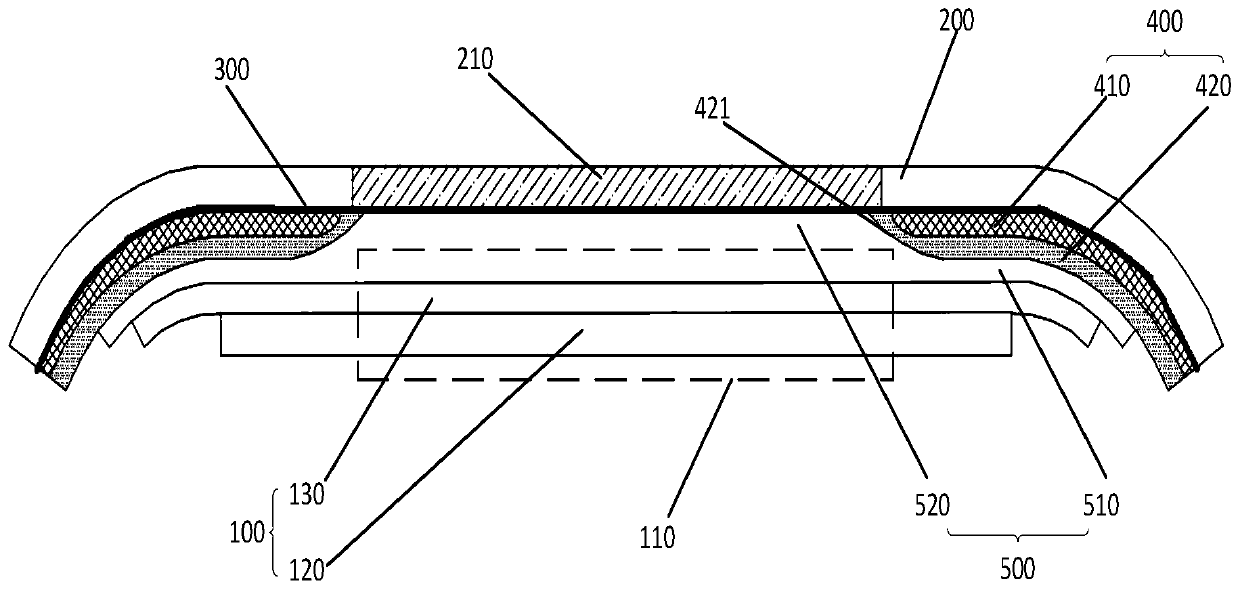
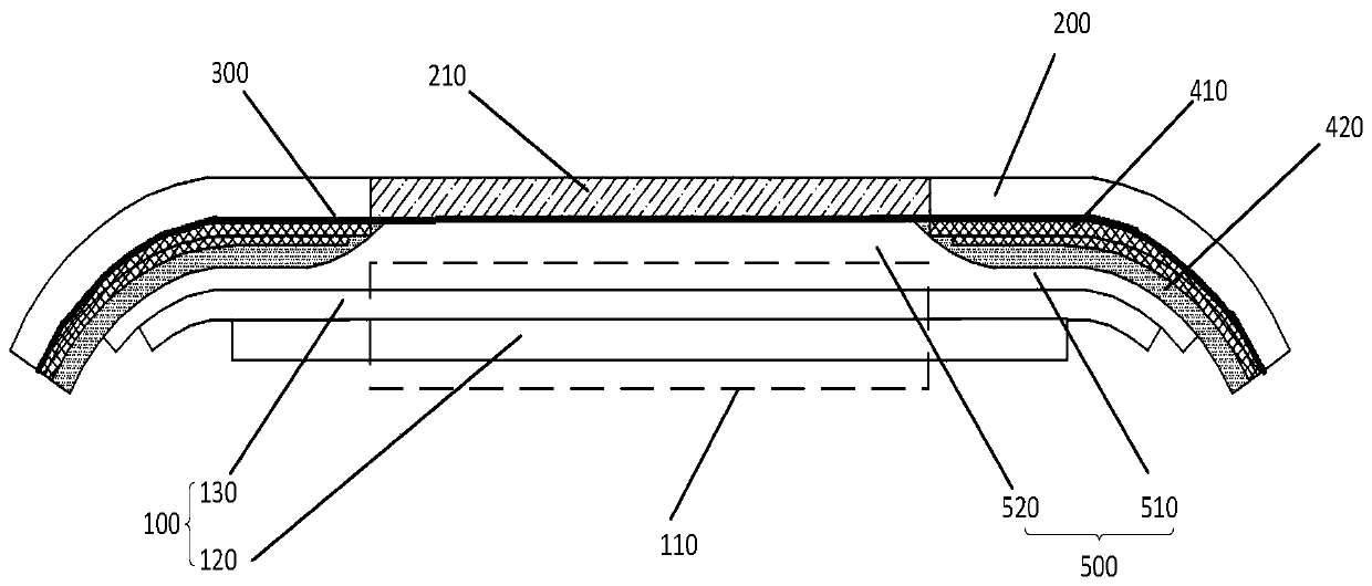
[0029] figure 2 Schematic diagram of the structure of the display screen device provided by the embodiment of the present invention, such as figure 2 As shown, in order to solve the problem that the ink layer 400 is easy to fall off caused by the direct soft and hard way between the ink layer 400 and the display module 100 or the curved protective cover 200 in the prior art, the embodiment of the present inv...
PUM
| Property | Measurement | Unit |
|---|---|---|
| thickness | aaaaa | aaaaa |
| thickness | aaaaa | aaaaa |
Abstract
Description
Claims
Application Information
 - R&D Engineer
- R&D Manager
- IP Professional
- Industry Leading Data Capabilities
- Powerful AI technology
- Patent DNA Extraction
Browse by: Latest US Patents, China's latest patents, Technical Efficacy Thesaurus, Application Domain, Technology Topic.
© 2024 PatSnap. All rights reserved.Legal|Privacy policy|Modern Slavery Act Transparency Statement|Sitemap