Touch display panel with fingerprint recognition function and touch display device

A technology of touch display panel and fingerprint recognition, which is applied in character and pattern recognition, acquisition/organization of fingerprint/palmprint, input/output process of data processing, etc. It can solve the problem of low recognition rate and recognition speed and technical difficulties of ultrasonic sensors and other issues, to achieve high industrial utilization and remarkable creative effects

Pending Publication Date: 2020-06-05
WUHAN CHINA STAR OPTOELECTRONICS SEMICON DISPLAY TECH CO LTD
View PDF11 Cites 8 Cited by
  • Summary
  • Abstract
  • Description
  • Claims
  • Application Information

AI Technical Summary

Problems solved by technology

These three fingerprint recognition technologies all use the ridges and valleys of the fingerprint to produce different feedback effects on the same detection signal. Among them, the ultrasonic sensor has the problem of low recognition rate and recognition speed, while the optical fingerprint recognition is due to its relatively high The large-volume optical system is difficult to adopt such a large optical system for devices with small thickness such as smart phones. The capacitive fingerprint recognition in the prior art usually adopts the method of plug-in to collect user fingerprint information, and the recognition module is additionally Designed outside the touch screen, such as the Home button of the mobile phone or the back of the fuselage, there are technical difficulties in integrating the fingerprint recognition matrix into the touch screen

Method used


Image

  • Touch display panel with fingerprint recognition function and touch display device
  • Touch display panel with fingerprint recognition function and touch display device
  • Touch display panel with fingerprint recognition function and touch display device

Examples


Embodiment Construction

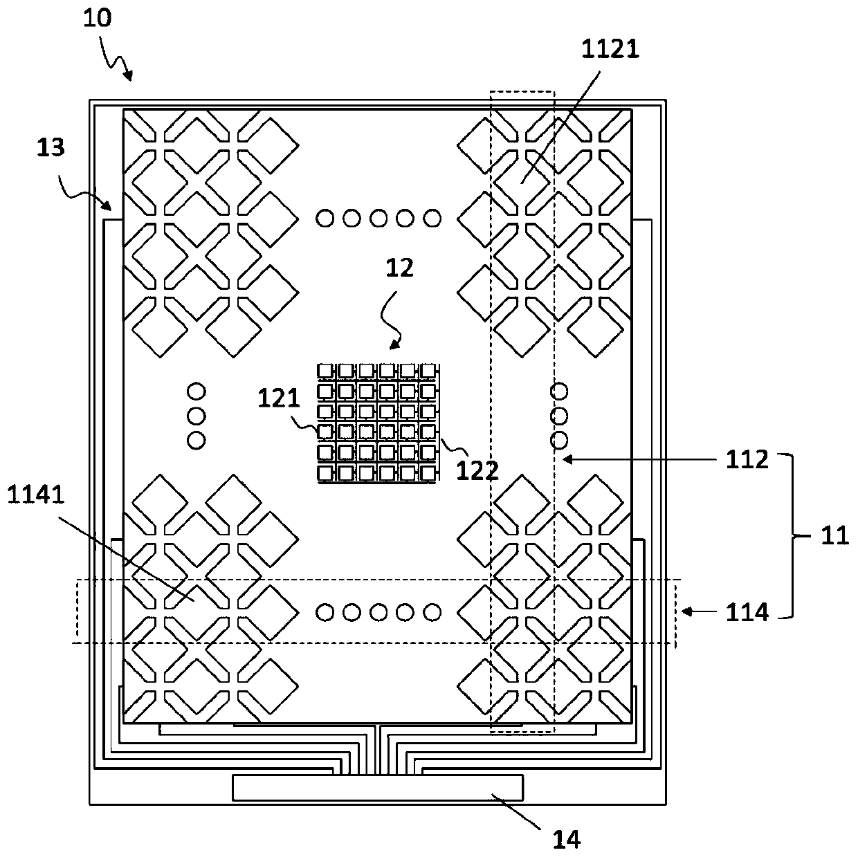
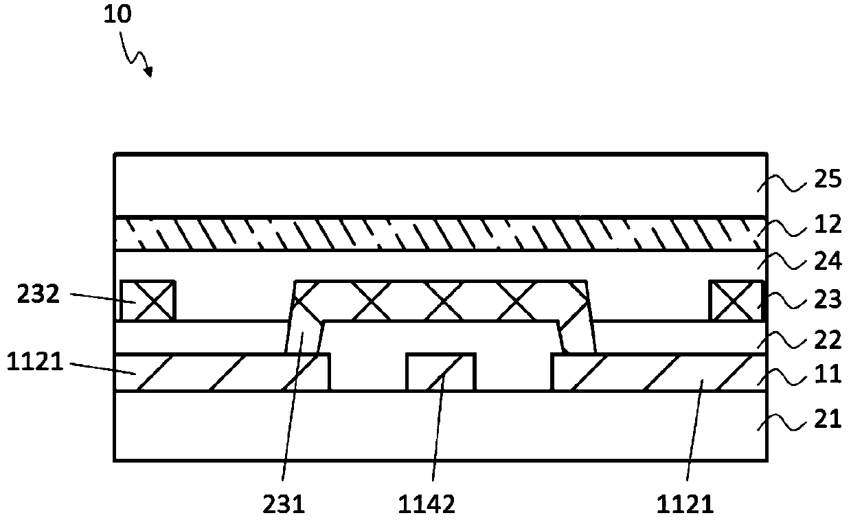
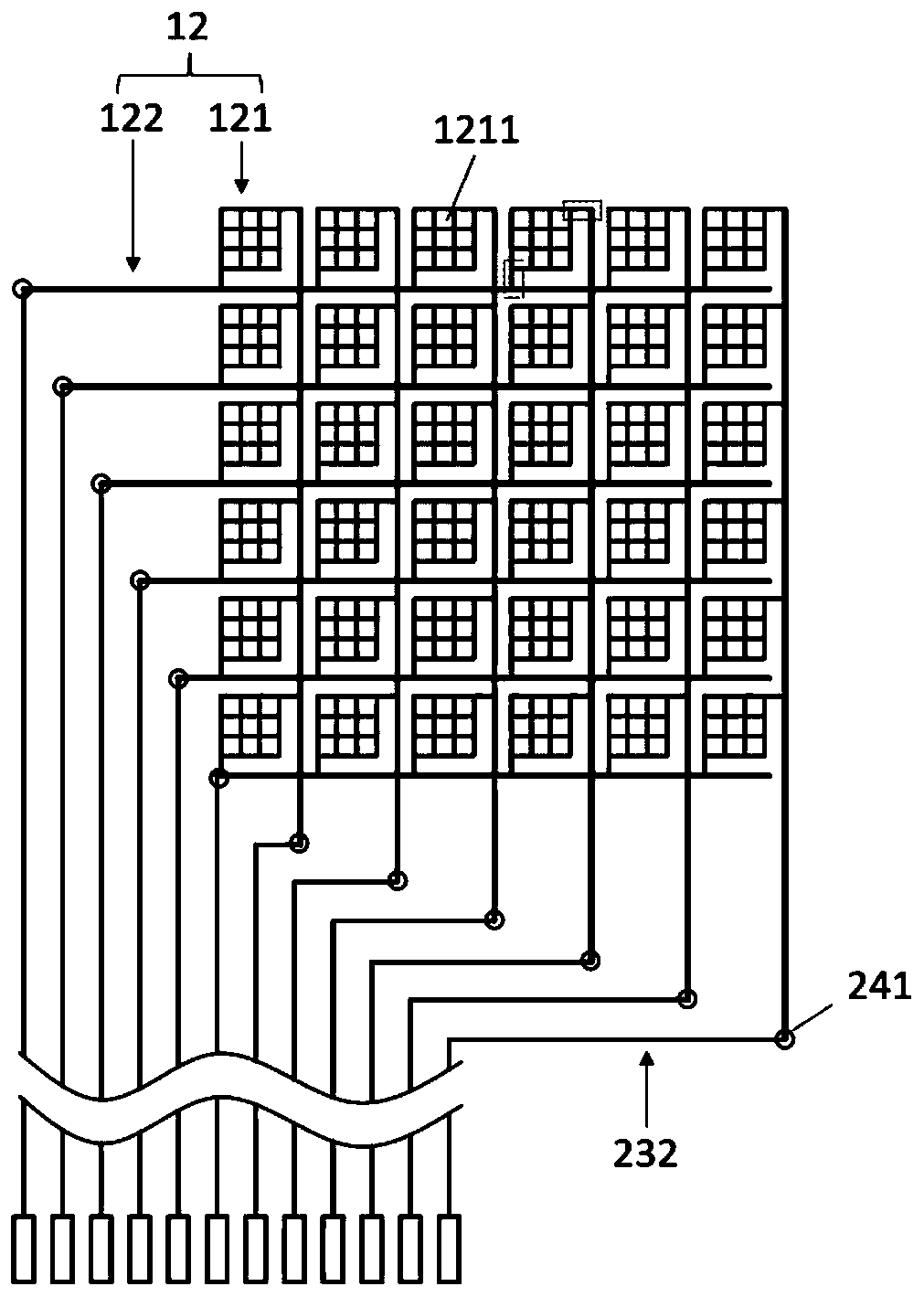
[0027] In order to make the object, technical solution and effect of the present invention more clear and definite, the present invention will be further described in detail below with reference to the accompanying drawings and examples. It should be understood that the specific embodiments described here are only used to explain the present invention, and the word "embodiment" used in the description of the present invention is intended to be used as an example or illustration, and should not be construed as limiting the present invention. Additionally, the terminology used herein is for the purpose of describing particular embodiments only and is not intended to be limiting of the exemplary embodiments. As used herein, the singular form "a" and "an" is also meant to include plural forms unless the context clearly dictates otherwise.

[0028] In the description of the present invention, it should be understood that the orientation or positional relationship indicated by the t...


PUM

PropertyMeasurementUnit
sizeaaaaaaaaaa
sizeaaaaaaaaaa

Abstract

The invention provides a touch display panel with a fingerprint recognition function. The touch display panel comprises a substrate, and a touch electrode, a first insulating layer, a conductive layer, a second insulating layer, a fingerprint identification layer and a protective layer which are sequentially arranged on the substrate, wherein the fingerprint identification layer is a conductor grid with high light transmittance, which is formed by arranging a plurality of wires in a staggered manner; the fingerprint identification layer comprises a plurality of fingerprint identification leads; the conductive layer comprises a plurality of fingerprint identification wires. Fingerprint identification can be integrated in the touch display panel through the conductor grid with high light transmittance without influencing display, and the second insulating layer is provided with the via hole, so that the plurality of fingerprint identification leads are electrically connected with the plurality of fingerprint identification wires, and the conductive layer is utilized to the greatest extent.

Description

technical field [0001] The invention relates to the field of fingerprint identification, in particular to a touch display panel and a touch display device with a fingerprint identification function. Background technique [0002] The current fingerprint recognition technology is mainly divided into three types: ultrasonic fingerprint recognition, optical fingerprint recognition and capacitive fingerprint recognition. These three fingerprint recognition technologies all use the ridges and valleys of the fingerprint to produce different feedback effects on the same detection signal. Among them, the ultrasonic sensor has the problem of low recognition rate and recognition speed, while the optical fingerprint recognition is due to its relatively high The large-volume optical system is difficult to adopt such a large optical system for devices with small thickness such as smart phones. The capacitive fingerprint recognition in the prior art usually adopts the method of plug-in to ...

Claims


Application Information

Patent Timeline
Patent Type & Authority Applications(China)
IPC IPC(8): G06F3/041G06F3/044G06K9/00
CPCG06F3/0412G06F3/0416G06F3/044G06F2203/04106G06V40/1306G06F3/0446G06F3/0443G06F2203/04111G06V10/17
Inventor 冯校亮
Owner WUHAN CHINA STAR OPTOELECTRONICS SEMICON DISPLAY TECH CO LTD
Why Eureka
Try Eureka