Eureka AIR delivers breakthrough ideas for toughest innovation challenges, trusted by R&D personnel around the world.

A kind of out-of-plane highly oriented cufesb film preparation method

A thin film preparation and orientation technology, which is applied in vacuum evaporation coating, coating, sputtering coating, etc., can solve the problems of not achieving obvious control effect and single control means

Active Publication Date: 2021-10-08
SHANGHAI INST OF MICROSYSTEM & INFORMATION TECH CHINESE ACAD OF SCI
View PDF3 Cites 0 Cited by
  • Summary
  • Abstract
  • Description
  • Claims
  • Application Information

AI Technical Summary

Problems solved by technology

[0005] At present, the research on the physical properties and regulation of CuFeSb is mainly carried out on polycrystalline samples. Doping chemical elements on polycrystalline samples is the most important method of regulation. The regulation method is single, and no obvious regulation effect has been achieved yet.
Experimentally, it is also impossible to perform multi-dimensional external field regulation on polycrystalline samples. For example, while introducing substrate stress to modulate the physical properties of the film, the gate voltage is applied to the film sample to introduce electric field effects.

Method used


Image

  • A kind of out-of-plane highly oriented cufesb film preparation method
  • A kind of out-of-plane highly oriented cufesb film preparation method
  • A kind of out-of-plane highly oriented cufesb film preparation method

Examples


Embodiment

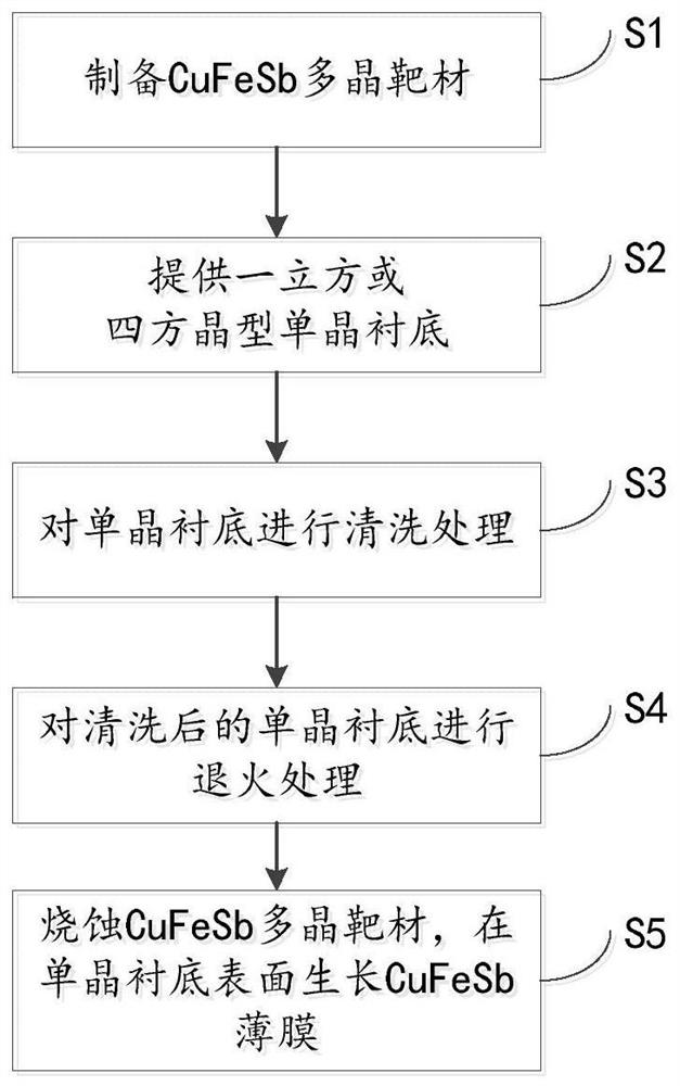
[0047] The embodiment of the present invention provides a method for preparing an out-of-plane highly oriented CuFeSb film, such as figure 1 As shown, the method includes the following steps:

[0048] S1. Prepare CuFeSb polycrystalline target;

[0049] S2. Provide a cubic or tetragonal single crystal substrate;

[0050] S3. Cleaning the single crystal substrate;

[0051] S4. Annealing the cleaned single crystal substrate;

[0052] S5. Ablating the CuFeSb polycrystalline target, and growing a CuFeSb thin film on the surface of the single crystal substrate.

[0053] In the embodiment of the present invention, the basic principle and process of using the pulsed laser deposition method to prepare thin films is that the focused laser beam interacts with the target to generate plasma, and the plasma is transported in space to form a highly oriented plume, which carries The high-energy particles condense on the substrate to form a thin film. Therefore, the acquisition of the tar...


PUM


Abstract

The invention discloses a method for preparing an out-of-plane highly oriented CuFeSb thin film. The method comprises the following steps: S1. preparing a CuFeSb polycrystalline target; S2. providing a cubic or tetragonal crystal substrate; S3. cleaning the crystal substrate; S4. performing annealing treatment on the cleaned single crystal substrate; S5. ablating the CuFeSb polycrystalline target, and growing a CuFeSb thin film on the surface of the single crystal substrate. The present invention utilizes pulsed laser deposition technology, through high-vacuum equipment, excimer laser hardware, synthesis of polycrystalline targets, selection of substrates, treatment of substrates, and stable control of film synthesis parameters, to prepare highly oriented CuFeSb out of plane The thin film is helpful to promote the research on the physical properties of CuFeSb, and the thin film has great advantages over polycrystalline materials, which expands the means of controlling the physical properties of CuFeSb, and is of great value to the material in basic research and magnetic material applications.

Description

technical field [0001] The invention relates to the field of material synthesis, in particular to a method for preparing an out-of-plane highly oriented CuFeSb thin film. Background technique [0002] Iron-based superconductors are the second largest family of high-temperature superconductors after copper-based high-temperature superconductors discovered in 2008. Its discovery broke the myth that iron elements are not conducive to the formation of superconductivity. The crystal structure, magnetic structure and electronic state diagram of the iron-based superconductor system and the copper-based superconductor are very similar, especially the structure of the iron-based superconductor is similar to the copper-oxygen plane of the high-temperature superconductor, and superconductivity occurs on the iron-based plane , a two-dimensional superconducting material. Therefore, the research on iron-based superconductivity will help to promote the solution process of high-temperature...

Claims


Application Information

Patent Timeline
Patent Type & Authority Patents(China)
IPC IPC(8): C23C14/28C23C14/18C23C14/02C22C30/02C22C1/04
CPCC22C1/04C22C30/02C23C14/02C23C14/18C23C14/28
Inventor 李卓君牟刚徐丽璇季秋骋宋叶凯彭炜
Owner SHANGHAI INST OF MICROSYSTEM & INFORMATION TECH CHINESE ACAD OF SCI
Why Eureka
Eureka Blog
Learn More