Check patentability & draft patents in minutes with Patsnap Eureka AI!

Flash memory unit and manufacturing method thereof

A manufacturing method and technology of flash memory cells, which are applied to electrical components, electric solid devices, circuits, etc., can solve problems such as insufficient coverage of contact etching stop layers, failure to store data in flash memory cells, etc., to solve data storage failures and improve coverage Insufficient effect

Pending Publication Date: 2020-11-13
NEXCHIP SEMICON CO LTD
View PDF11 Cites 0 Cited by
  • Summary
  • Abstract
  • Description
  • Claims
  • Application Information

AI Technical Summary

Problems solved by technology

[0005] The purpose of the present invention is to provide a flash memory unit and its manufacturing method to solve the problem that the bottom of the isolation sidewall is insufficiently covered by the contact etch stop layer, and then block the sodium ions generated in the back-end process from entering the isolation sidewall, and solve the problem of the flash memory unit. Data save failure problem

Method used


Image

  • Flash memory unit and manufacturing method thereof
  • Flash memory unit and manufacturing method thereof
  • Flash memory unit and manufacturing method thereof

Examples


Embodiment Construction

[0042] The flash memory unit and its manufacturing method proposed by the present invention will be further described in detail below with reference to the drawings and specific embodiments. The advantages and features of the present invention will be more apparent from the following description. It should be noted that all the drawings are in a very simplified form and use imprecise scales, and are only used to facilitate and clearly assist the purpose of illustrating the embodiments of the present invention.

[0043] refer to figure 1 , the manufacturing method of a kind of Nor type flash memory unit comprises at present:

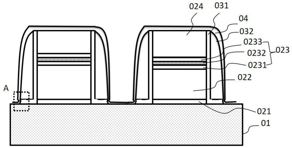
[0044] Step S1: providing a base, and the base includes a substrate 01, a gate structure located above the substrate 01, and isolation spacers located on both sides of the gate structure, wherein the gate structure includes A tunnel dielectric layer 021, a floating gate layer 022, an ONO dielectric layer 023, and a control gate layer 024 are stacked in ...


PUM

PropertyMeasurementUnit
Thicknessaaaaaaaaaa

Abstract

The invention provides a flash memory unit and a manufacturing method thereof. The manufacturing method of the flash memory unit comprises the steps of firstly, providing a substrate with an isolationside wall, wherein a recess exists in the bottom of the isolation side wall; then forming a first contact etching stop layer on the substrate, and filling the recess with the first contact etching stop layer; secondly, etching the first contact etching stop layer, and reserving the first contact etching stop layer in the recess; and finally, forming a second contact etching stop layer on the substrate and the first contact etching stop layer in the recess. By forming the contact etching stop layer twice, the problem that the bottom of the isolation side wall is insufficiently covered can be solved, and then the problem of data storage failure of the flash memory unit can be solved.

Description

technical field [0001] The invention relates to the field of semiconductor manufacturing, in particular to a flash memory unit and a manufacturing method thereof. Background technique [0002] Flash memory is a widely used non-volatile computer storage technology, which usually uses a floating gate or charge trapping structure to store charges in field effect transistors to form a memory unit. [0003] According to the difference between the logic gates during the read operation, there are two types of flash memory: NAND type and NOR type. NOR flash memory can perform independent read and write operations for each of its storage units, providing complete random access functions, so it can be used for non-volatile storage of executable programs and can replace volatile SRAM and DRAM. Moreover, NOR-type flash memory has great technical advantages over NAND-type flash memory: it provides a general-purpose non-volatile memory with complete random access function, which can be u...

Claims


Application Information

Patent Timeline
IPC IPC(8): H01L27/11517H01L27/11521
CPCH10B41/00H10B41/30
Inventor 操梦雅金起準
Owner NEXCHIP SEMICON CO LTD
Features
  • R&D
  • Intellectual Property
  • Life Sciences
  • Materials
  • Tech Scout
  • Unparalleled Data Quality
  • Higher Quality Content
  • 60% Fewer Hallucinations
Learn More