Solder mask manufacturing method of thick copper circuit board

A technology of thick copper circuit board and manufacturing method, which is applied in the directions of printed circuit manufacturing, printed circuit, printed circuit secondary treatment, etc., can solve problems such as difficulty in filling gaps, and achieve the effect of avoiding quality problems

Inactive Publication Date: 2020-12-15
鹤山市中富兴业电路有限公司
View PDF6 Cites 4 Cited by
  • Summary
  • Abstract
  • Description
  • Claims
  • Application Information

AI Technical Summary

Problems solved by technology

[0003] The purpose of the present invention is to at least solve one of the technical problems existing in the prior art, and provide a method for manufacturing thick copper circuit board solder resist, which can overcome the disadvantage of difficulty in filling gaps caused by one-time silk screen printing

Method used


Image

  • Solder mask manufacturing method of thick copper circuit board
  • Solder mask manufacturing method of thick copper circuit board
  • Solder mask manufacturing method of thick copper circuit board

Examples


Embodiment Construction

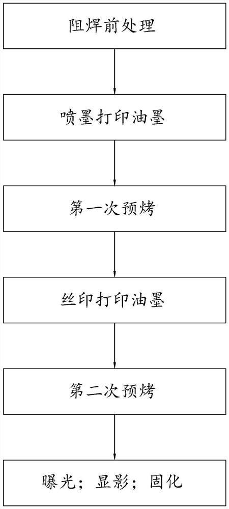
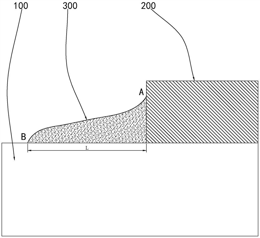
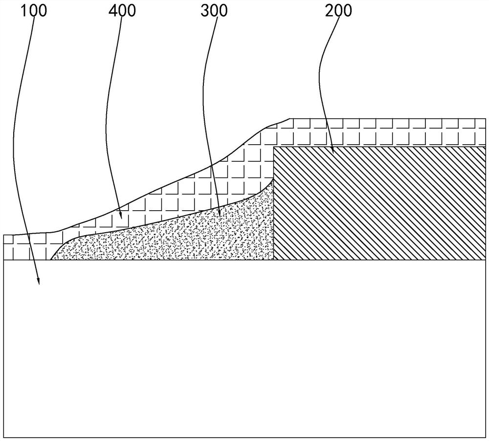
[0026] This part will describe the specific embodiment of the present invention in detail, and the preferred embodiment of the present invention is shown in the accompanying drawings. Each technical feature and overall technical solution of the invention, but it should not be understood as a limitation on the protection scope of the present invention.

[0027] In the description of the present invention, it should be understood that the orientation descriptions, such as up, down, front, back, left, right, etc. indicated orientations or positional relationships are based on the orientations or positional relationships shown in the drawings, and are only In order to facilitate the description of the present invention and simplify the description, it does not indicate or imply that the device or element referred to must have a specific orientation, be constructed and operated in a specific orientation, and thus should not be construed as limiting the present invention.

[0028] I...


PUM


Abstract

The invention discloses a resistance welding manufacturing method of a thick copper circuit board. The resistance welding manufacturing method comprises the following steps of resistance welding pretreatment, forming a thick copper layer on a base material; ink-jet printing, filling solder resist green oil in seams and corners between the thick copper layer and the base material; pre-baking for the first time, pre-baking the solder resist green oil to enable the solder resist green oil to lose liquidity; silk-screen printing of printing ink, silk-screen printing of solder mask being carried out on the surfaces of the base material, the thick copper layer and the solder mask green oil; pre-baking for the second time, pre-baking the silk-screen printing ink to enable the silk-screen printingink to lose liquidity; performing exposure; developing being performed; curing. Ink-jet printing is adopted to fill green oil in difficult-to-fill steps and gaps such as line gaps and corners of a thick copper layer and a base material, printing ink only needs to be printed in a silk-screen mode once after pre-baking, the defect that gaps are difficult to fill due to one-time silk-screen printingcan be overcome, repeated silk-screen solder resist does not need to be conducted, and ink viscosity does not need to be changed. The method is advantaged in that various quality problems are avoided.

Description

technical field [0001] The invention relates to the technical field of printed circuit boards, in particular to a solder resist manufacturing method for thick copper circuit boards. Background technique [0002] Generally, the finished copper thickness of the outer layer ≥ 2Oz is defined as a thick copper plate. Thick copper plates are mainly used for power circuit boards and high-power circuits that require large currents. For thick copper plates, due to the large gap between the base material and the line surface, it is difficult to fill the gaps with solder mask. If the viscosity of the ink is too high in order to meet the thickness of the solder mask on the line surface, it will be difficult to apply oil to fill the lines, corners, and seams between the copper and the substrate, and there will be problems such as easy oil accumulation and many air bubbles; if In order to fill the gap, if the ink viscosity is adjusted too low, it will be difficult to meet the printing t...

Claims


Application Information

Patent Timeline
Patent Type & Authority Applications(China)
IPC IPC(8): H05K3/28
CPCH05K3/282
Inventor 叶国俊
Owner 鹤山市中富兴业电路有限公司
Why Eureka
Try Eureka