Eureka AIR delivers breakthrough ideas for toughest innovation challenges, trusted by R&D personnel around the world.

LED lamp bead plate, manufacturing method thereof and display panel

A technology of LED lamp beads and manufacturing methods, which is applied in the direction of electrical components, electric solid devices, circuits, etc., can solve the problems of poor heat dissipation, etc., and achieve the goal of improving the overall brightness, improving the light mixing efficiency, and reducing the light mixing distance between lamps Effect

Pending Publication Date: 2021-02-05
HUIZHOU JUFEI OPTOELECTRONICS CO LTD
View PDF5 Cites 2 Cited by
  • Summary
  • Abstract
  • Description
  • Claims
  • Application Information

AI Technical Summary

Problems solved by technology

In this technology, it is also necessary to fill conductors in the connected through holes and blind holes. The heat generated by the LED chip on the PCB is mainly dissipated through the conductors, and the heat dissipation performance is relatively poor.

Method used


Image

  • LED lamp bead plate, manufacturing method thereof and display panel
  • LED lamp bead plate, manufacturing method thereof and display panel
  • LED lamp bead plate, manufacturing method thereof and display panel

Examples


Embodiment Construction

[0064] In order to make the object, technical solution and advantages of the present invention clearer, the embodiments of the present invention will be further described in detail below through specific implementation manners in conjunction with the accompanying drawings. It should be understood that the specific embodiments described here are only used to explain the present invention, not to limit the present invention.

[0065] This embodiment provides an LED lamp bead board with low technical difficulty, easy mass production and good heat dissipation performance. In order to facilitate understanding, this embodiment will exemplify the manufacturing method of the LED lamp bead board below.

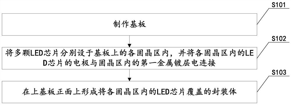
[0066] See figure 1 As shown, the manufacturing method of the LED lamp bead board exemplified in this embodiment may include but not limited to:

[0067] S101: making a substrate.

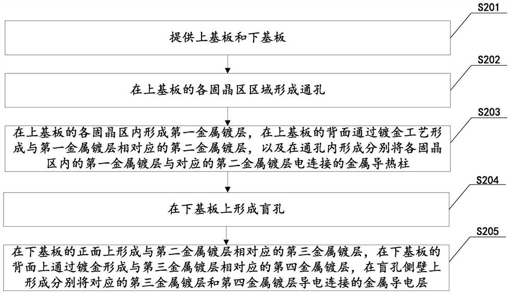
[0068] In an example of this embodiment, S101 refers to figure 2 shown, including but not limited to...


PUM


Abstract

The invention provides an LED lamp bead board and a manufacturing method thereof, and a display panel. An upper substrate and a lower substrate are combined to form a substrate; through holes are independently formed in the upper substrate, blind holes are independently formed in the lower substrate, a mature process can be adopted, metal heat conduction columns are arranged in the through holes,the metal conducting layers are formed in the blind holes and the corresponding metal coatings are formed on the upper substrate and the substrate. the universality is good, implementation is easy, efficiency and yield are high, cost is low, and mass production, popularization and application are easy; compared with a single-layer substrate with the same thickness, the substrate formed by the upper substrate and the lower substrate has the advantages that the height of the metal heat conduction columns is only half of or even smaller than the height of the metal heat conduction columns, used for enabling heat generated by the LED chips to be generated everywhere, in the single-layer substrate, so that heat dissipation paths can be greatly reduced, and the heat dissipation performance is better.

Description

technical field [0001] The invention relates to the field of light-emitting diodes, in particular to an LED lamp bead board, a manufacturing method thereof, and a display panel. Background technique [0002] At present, mobile communication terminals such as laptops, tablets, and mobile phones have higher and higher color gamut and brightness requirements for backlight light sources, and the thickness is getting thinner and thinner. The original bracket-type LED light source has gradually been unable to meet this small size, high brightness requirements. Therefore, in order to reduce the size of the bracket-type LED bead light source, a substrate-type LED light source has been proposed in the industry. This technology requires forming blind holes on a single-layer substrate and forming through holes communicating with the blind holes at corresponding blind hole positions. Through holes and blind holes are drilled from the front and back of the single-layer substrate respec...

Claims


Application Information

Patent Timeline
IPC IPC(8): H01L25/075H01L33/48H01L33/54H01L33/62H01L33/64
CPCH01L25/0753H01L33/483H01L33/62H01L33/54H01L33/642H01L2933/0033H01L2933/0066
Inventor 胡永恒项文斗刘乐鹏李运华梁海志孙平如邢美正
Owner HUIZHOU JUFEI OPTOELECTRONICS CO LTD
Why Eureka
Eureka Blog
Learn More