Novel HIT and EB material matched organic light-emitting device

An electroluminescent device and electroluminescent technology, applied in the field of semiconductors, can solve the problems of large HOMO energy level difference, affecting device performance, affecting device life, etc.

CN112490376AActive Publication Date: 2021-03-12JIANGSU SUNERA TECH CO LTD
3 Cites 1 Cited by

Patent Information

Authority / Receiving Office
CN · China
Current Assignee / Owner
Publication Date
2021-03-12

Smart Images

  • Figure 1
    Figure 1
  • Figure 2
    Figure 2
  • Figure 3
    Figure 3
Patent Text Reader

Abstract

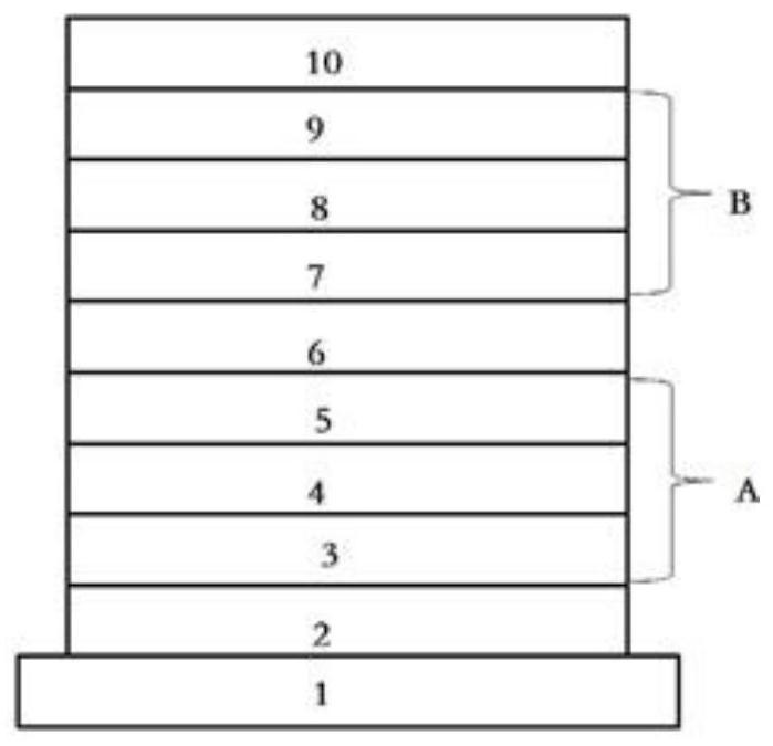
The invention discloses a novel HIT and EB material matched organic light-emitting device, which is sequentially provided with a substrate, a first electrode, an organic functional material layer anda second electrode from bottom to top, and is characterized in that the organic functional material layer comprises: a hole transport region located on the first electrode; a light-emitting layer overthe hole transport region, the light-emitting layer including a host material and a guest material; and an electron transmission region which is located on the light-emitting layer. The hole transport region sequentially comprises a hole injection layer, a hole transport layer and an electron blocking layer from bottom to top, the hole injection layer comprises a hole transport layer material anda P-type doped material, and the hole transport layer comprises an organic compound containing dimethyl fluorenyl in the structure. The electron blocking layer comprises an organic electroluminescentdevice having improved luminous efficiency and lifespan, and a display comprising the same, and more particularly, to an organic electroluminescent device having improved luminous efficiency and lifespan, and an electronic device comprising the same.
Need to check novelty before this filing date? Find Prior Art

Description

technical field

[0001] The invention relates to the technical field of semiconductors, in particular to a novel organic electroluminescent device with a combination of HIT and EB materials and a display comprising the same. Background technique

[0002] Organic electroluminescence (OLED: Organic Light Emitting Diodes) device technology can be used to manufacture new display products, and can also be used to make new lighting products. It is expected to replace the existing liquid crystal display and fluorescent lighting, and has a wide application prospect. Typically, an OLED is composed of several layers including a positive electrode, a negative electrode, a hole injection layer, a hole transport layer, an organic light emitting layer, an electron transport layer, and an electron injection layer. OLED light-emitting device is a current device. When a voltage is applied to the electrodes at its two ends, and the positive and negative charges in the organic layer functional ...

Examples

preparation Embodiment 1

[0109] Hole injection layer 1: Use the OLED Chuster Deposition System (manufacturer: CHOSHU INDUSTRY Co.LTD.) evaporation equipment of model 1504-10117-01-0 to place the hole transport host material HI1 and the P-type dopant material P1 on the Two evaporation sources, at a vacuum degree of 1.0E -5 Under Pa pressure, control the evaporation rate of HIT1 as Control the evaporation rate of P-type dopant material 1 as Co-distilled together to obtain HI1 of the present invention.

[0110] Hole injection layer 2: repeat the preparation process of hole injection layer preparation example 1, the difference is that HIT1 is replaced by HIT3 to obtain HI2.

[0111] Hole injection layer 3: Repeat the preparation process of hole injection layer preparation example 1, except that HIT1 is replaced by HIT11 to obtain HI3.

[0112] Hole injection layer 4: Repeat the preparation process of hole injection layer preparation example 1, except that HIT1 is replaced by HIT15 to obtain HI4.

[0...