Mini-LED display screen splicing display driving system and driving display method
A splicing display and drive system technology, applied in the direction of static indicators, instruments, etc., can solve the problems of limited cost or yield factor of large screens, and difficulty in popularization and application
- Summary
- Abstract
- Description
- Claims
- Application Information
AI Technical Summary
Problems solved by technology
Method used
Image
Examples
Embodiment 1
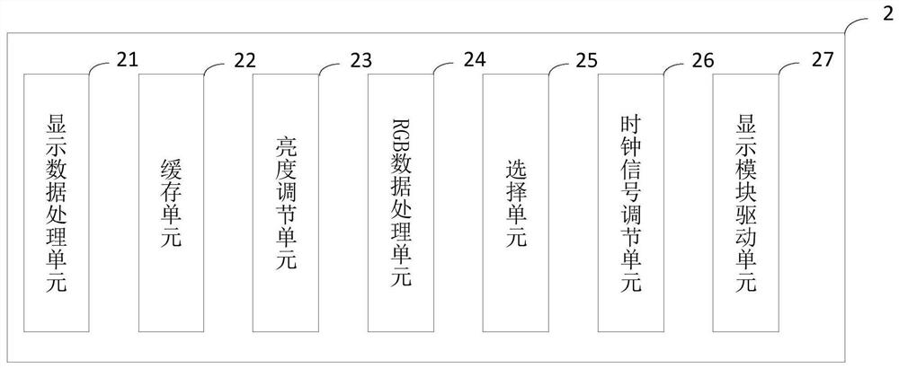
[0041] figure 1 The structural schematic diagram of the Mini-LED display splicing display drive system provided for the embodiment of this application includes: a storage module 1, a control module 2 and a Mini-LED display module 3, the storage module 1 is used to provide display data, and the The control module 2 is used to process the display data into a display signal and send it to the Mini-LED display module 3. The Mini-LED display module 3 receives the display signal to control the display of the Mini-LED display. The LED display module 3 is spliced by two or three Mini-LED display units. Specifically, the display unit has a resolution of 135*120, the size of the LED chips is 100 microns, and the spacing between the LED chips is 680 Micron Mini-LED display.
[0042] In this embodiment, the storage module 1 can be a memory card, preferably a micro SD card. This embodiment uses a micro SD card, which is more conducive to saving space. Specifically, the storage module 1...
Embodiment 2
[0081] This embodiment further proposes a driving display method for splicing display of two, three, six and eight Mini-LED screens, such as Image 6 As shown, the steps are as follows:
[0082] S100. The display data processing unit reads the display data from the SD card, and transmits the read data and address to the cache unit.
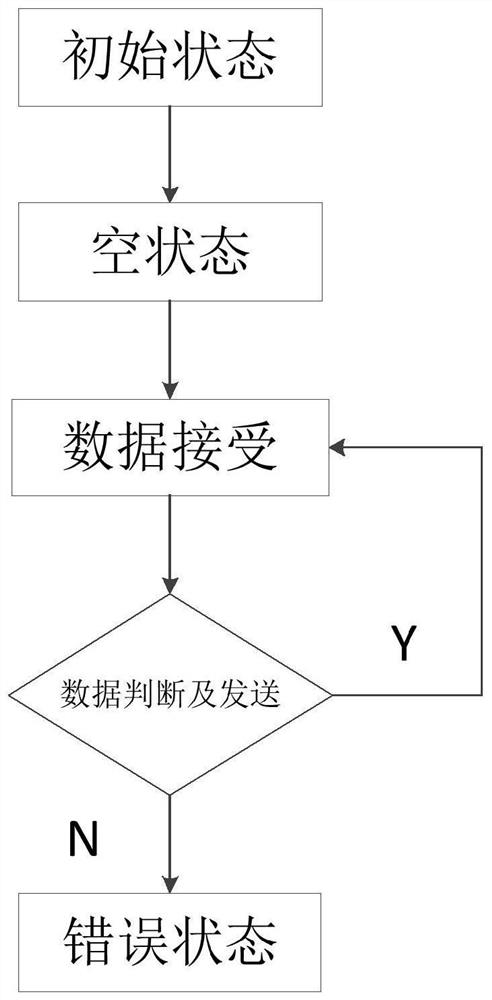
[0083] In this embodiment, the reading of display data is controlled according to SWITCH, and the SPI working mode (SD_CS signal is active at low level) is enabled for signal gating. The flow diagram is shown in image 3 and Figure 4 shown. The main logic is to use the state machine to perform each working state in SPI mode, including initialization (STATE_spi_init), empty state (STATE_spi_idle), transmission (STATE_spi_tx), transmission 1 (STATE_spi_tx1) and transmission 2 (STATE_spi_tx2). In the sending state, each rising edge of the clock accepts 1 bit data, and at least 8 clocks are required to transmit 8 bit data.
[0084] Secondly, acco...
PUM
 Abstract
Description
Claims
Application Information


