Display panel

A display panel and substrate technology, applied in the direction of instruments, identification devices, etc., can solve problems such as smearing, jumping of display elements, and poor interactivity, and achieve the effects of solving jumping and smearing, optimizing display effects, and strong interactivity

Pending Publication Date: 2021-05-14
JIHUA LAB
View PDF11 Cites 1 Cited by
  • Summary
  • Abstract
  • Description
  • Claims
  • Application Information

AI Technical Summary

Problems solved by technology

In the display panel production industry, the division of labor is clear and the system is complete. Under this mature and traditional production mode, the shortcomings of the display panel are also exposed.
[0003] Since the pixel structure and pixel driver are produced independently and then packaged, when several pixel structures are packaged on the panel substrate, it is necessary to reserve enough area to install the pixel driver, such as image 3 As shown, the general pixel structures 10 are arranged in an array distribution, and the area reserved between the pixel structures of two adjacent columns is installed for pixel driving, which makes the transition gap 20 between the pixel structures of two adjacent columns larger, resulting in During the display process of the display panel, jumping and smearing problems occur when the display elements are translated. Since each component is produced independently, it is difficult for the panel substrate factory to solve this problem by controlling the distance between the pixel structures during packaging.
Furthermore, in the existing display panel, among several pixel structures, the RGB sub-pixels are arranged in the same way, resulting in poor interaction between the sub-pixels of the pixel structure, and only a single pixel structure can be used as a pixel For display, when the display elements are translated, the distance between pixels is relatively large, which also highlights the problems of display jumping and smearing

Method used


Image

  • Display panel
  • Display panel
  • Display panel

Examples


Embodiment Construction

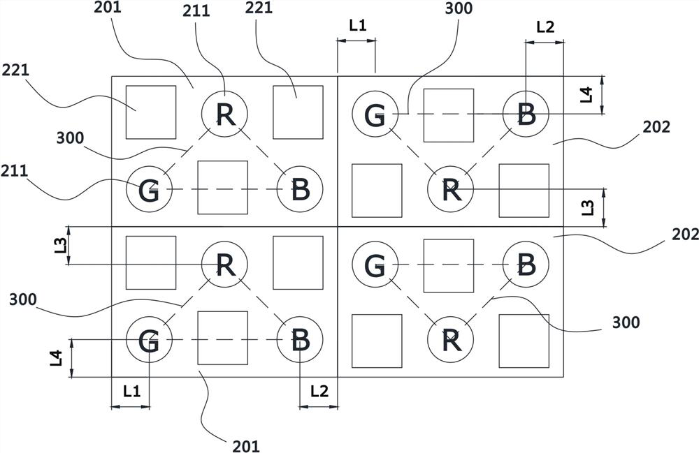
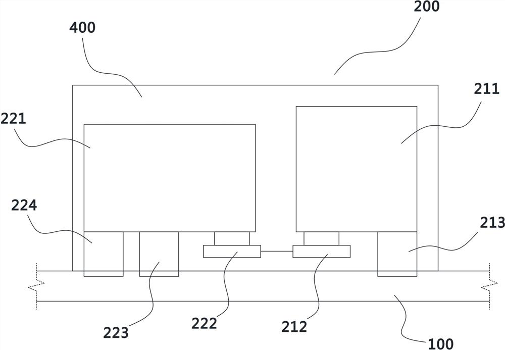
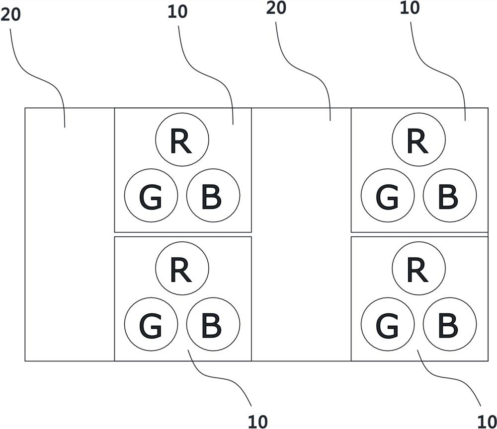
[0022] Embodiments of the present invention are described in detail below, examples of which are shown in the drawings, wherein the same or similar reference numerals denote the same or similar elements or elements having the same or similar functions throughout. The embodiments described below by referring to the figures are exemplary only for explaining the present invention and should not be construed as limiting the present invention.

[0023] In describing the present invention, it should be understood that the terms "center", "longitudinal", "transverse", "length", "width", "thickness", "upper", "lower", "front", " Orientation indicated by rear, left, right, vertical, horizontal, top, bottom, inside, outside, clockwise, counterclockwise, etc. The positional relationship is based on the orientation or positional relationship shown in the drawings, which is only for the convenience of describing the present invention and simplifying the description, rather than indicating ...


PUM


Abstract

The invention discloses a display panel. The display panel comprises a substrate; a plurality of pixel structures are distributed on the substrate in an array mode; the pixel structures are divided into first pixel structures and second pixel structures; the first pixel structures and the second pixel structures are in a mirror image mode along a vertical direction; in the pixel structures distributed in the array mode, the pixel structures in the odd-numbered columns are the first pixel structures, and the pixel structures in the even-numbered columns are the second pixel structures, or the pixel structures in the odd-numbered columns are second pixel structures, and the pixel structures in the even-numbered columns are first pixel structures; each of the first pixel structures and the second pixel structures comprises a pixel unit and a pixel driver which are integrally packaged; each pixel unit comprises three different sub-pixels, an isosceles triangle structure is formed among the three sub-pixels; and each pixel driver comprises three sub-drivers, and the three sub-drivers are electrically connected with the three sub-pixels respectively. According to the display panel provided by the invention, the problems of jumping and smear occurring during translation of the display elements can be effectively solved, and the display effect of the display panel is remarkably optimized.

Description

technical field [0001] The invention belongs to the field of display technology, in particular to a display panel. Background technique [0002] The display panel mainly includes three parts: pixel structure (generally including RGB sub-pixels), pixel driver and panel substrate. In the existing production process, the pixel structure is independently packaged and completed by the lamp bead manufacturer; the display panel manufacturer designs the panel row and column control scheme, prepares the driving substrate (specifically including installing the pixel driver on the panel substrate), and then packages the The lamp beads (that is, the pixel structure) are welded and processed to produce a finished display panel. In the display panel production industry, the division of labor in production is clear and the system is complete. Under this mature and traditional production mode, the shortcomings of display panels are also exposed. [0003] Since the pixel structure and pixe...

Claims


Application Information

Patent Timeline
Patent Type & Authority Applications(China)
IPC IPC(8): G09F9/302
CPCG09F9/302
Inventor 马宝真郑喜凤蔡炜张庆凯王铂曹慧张朝志
Owner JIHUA LAB
Why Eureka
Try Eureka