Double-sided circuit board and manufacturing method thereof

A technology of double-sided circuit board and manufacturing method, which is applied in the direction of printed circuit manufacturing, printed circuit, printed circuit components, etc. simple effect

Active Publication Date: 2021-07-02
BEIJING DREAM INK TECH CO LTD
View PDF13 Cites 1 Cited by
  • Summary
  • Abstract
  • Description
  • Claims
  • Application Information

AI Technical Summary

Problems solved by technology

[0004] In view of this, an object of the present invention is to propose a method for manufacturing double-sided circuit boards, so as to solve the problem that the manufacturing process of double-sided boards in the prior art cannot meet the production requirements of high-precision circuits.

Method used


Image

  • Double-sided circuit board and manufacturing method thereof
  • Double-sided circuit board and manufacturing method thereof
  • Double-sided circuit board and manufacturing method thereof

Examples


Embodiment Construction

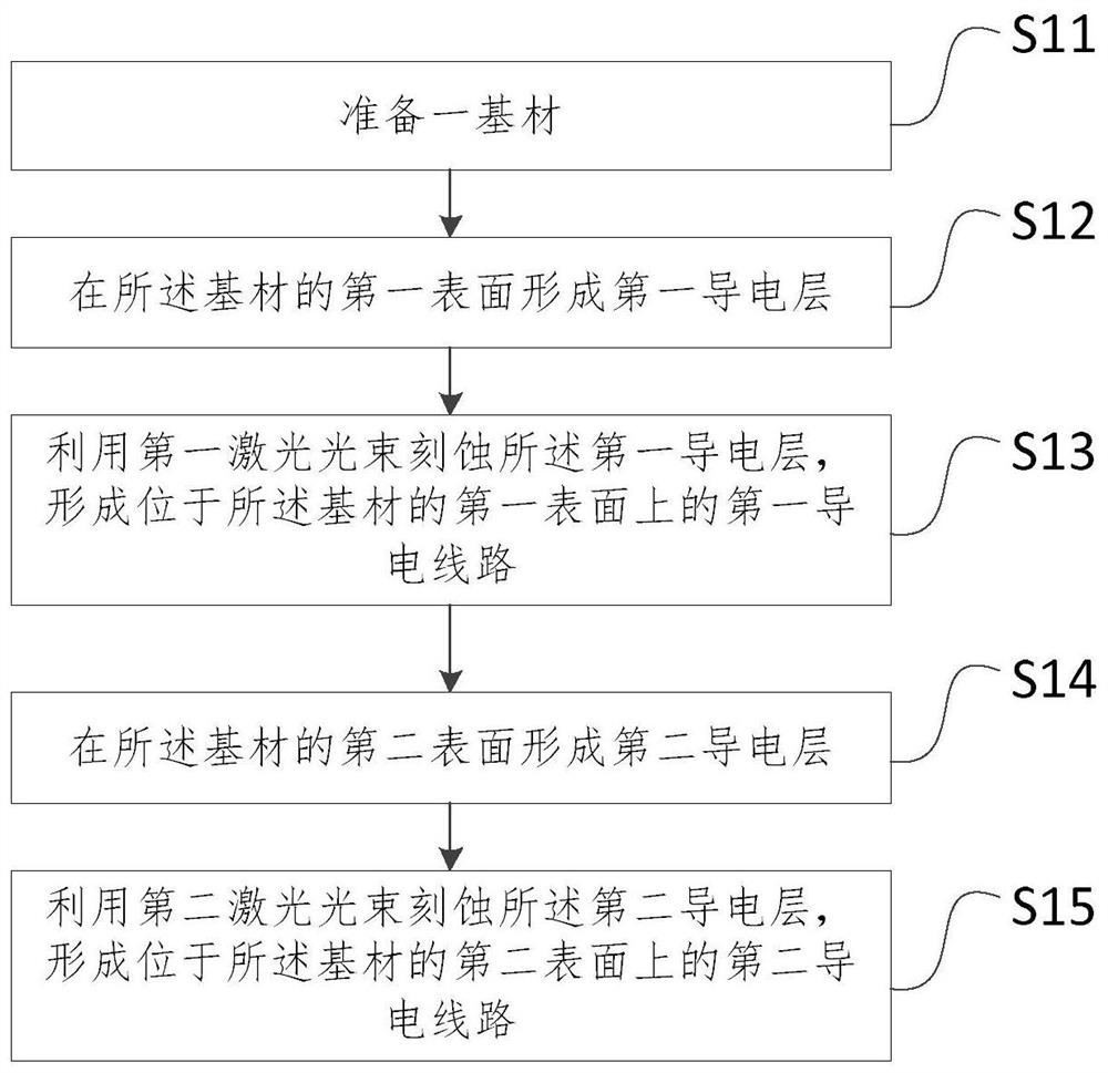
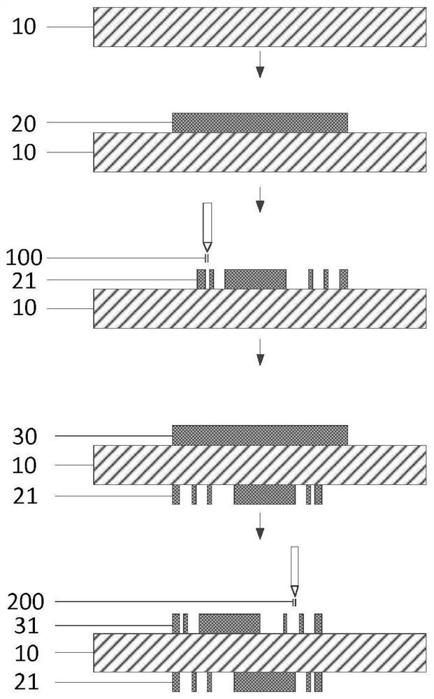
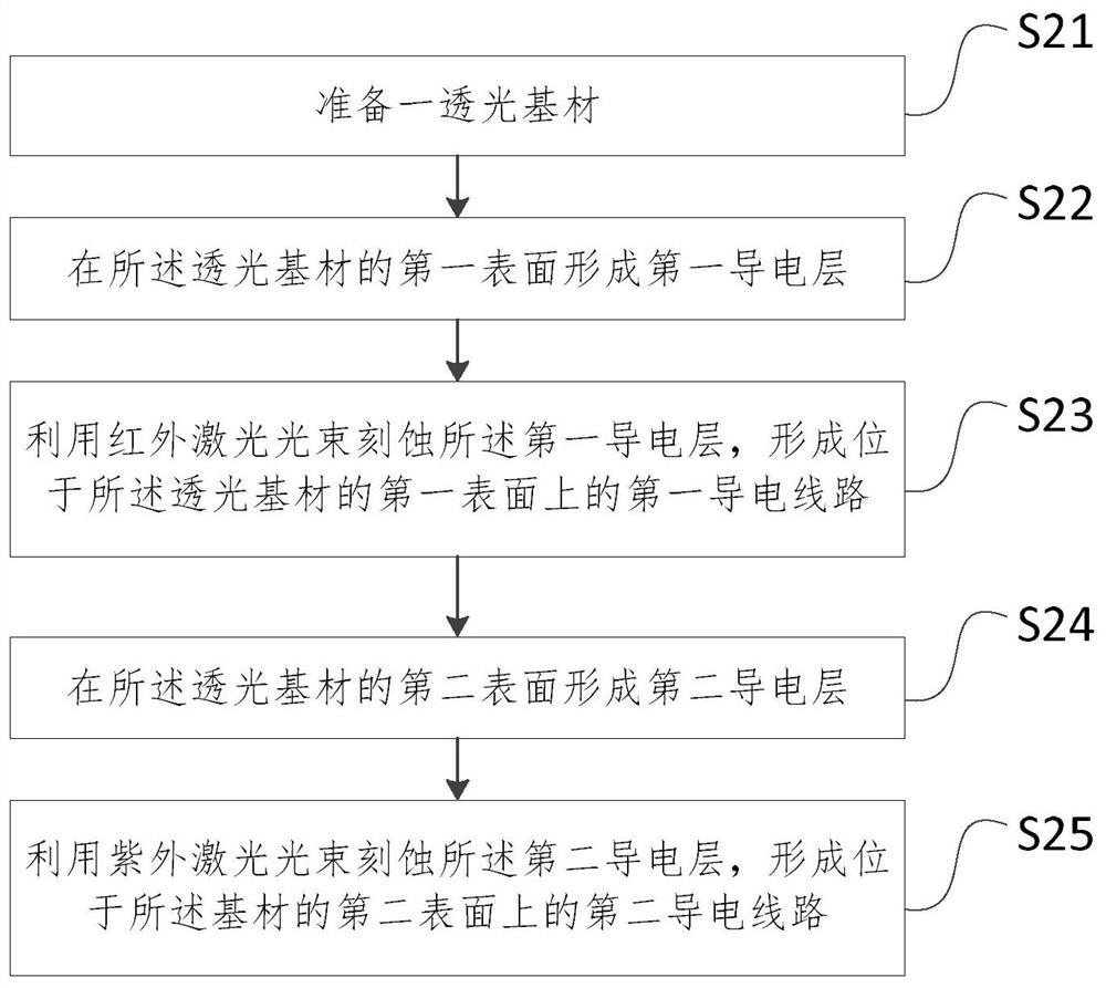
[0022] The following description and drawings illustrate specific embodiments of the invention sufficiently to enable those skilled in the art to practice them. Other embodiments may incorporate structural, logical, electrical, process, and other changes. The examples merely represent possible variations. Individual components and functions are optional unless explicitly required, and the order of operations may vary. Portions and features of some embodiments may be included in or substituted for those of other embodiments. The scope of embodiments of the present invention includes the full scope of the claims, and all available equivalents of the claims. These embodiments of the present invention may be referred to herein, individually or collectively, by the term "invention", which is for convenience only and is not intended to automatically limit the application if in fact more than one invention is disclosed The scope is any individual invention or inventive concept.

...


PUM

PropertyMeasurementUnit
melting pointaaaaaaaaaa
transmittivityaaaaaaaaaa

Abstract

The invention discloses a double-sided circuit board and a manufacturing method thereof, and relates to the technical field of electronic circuit preparation. The manufacturing method of the double-sided circuit board comprises the following steps: preparing a base material; forming a first conductive layer on the first surface of the base material; etching the first conductive layer by using a first laser beam to form a first conductive circuit located on the first surface of the base material; forming a second conductive layer on the second surface of the base material; and etching the second conductive layer by using a second laser beam to form a second conductive circuit on the second surface of the base material. According to the embodiment of the invention, the conductive layer is processed and formed on the substrate through the laser etching process, the high-precision circuit board can be manufactured by means of the high-precision performance of the laser beams, and the process is simple, high in plate making efficiency and capable of meeting the industrial plate making requirement.

Description

technical field [0001] The invention belongs to the technical field of electronic circuit production, and in particular relates to a double-sided circuit board and a production method thereof. Background technique [0002] With the development of high technology, people need electronic products with high performance, small size and multiple functions, which promotes the development of printed circuit board manufacturing to be light, thin, short and small, so that more functions can be realized by using limited space, and the wiring density will increase. , targets with smaller apertures. [0003] Double-sided circuit board (also known as double-sided board) refers to the interconnected circuit structure formed on both sides of the same substrate. The plate-making process of the double-sided board is mainly formed by etching the copper clad board through the traditional chemical etching process. Conductive lines, this process has problems such as complicated procedures, low ...

Claims


Application Information

Patent Timeline
Patent Type & Authority Applications(China)
IPC IPC(8): H05K3/02H05K1/11
CPCH05K3/027H05K1/11
Inventor 鲁强赵建慧赵先福吕文峰
Owner BEIJING DREAM INK TECH CO LTD
Why Eureka
Try Eureka