Sheet like variable resistor having metallic terminals

A resistor and variable technology, applied in the direction of sliding contact resistors, resistor terminals/electrodes, manufacturing resistor chips, etc., can solve the problem of non-volatile, unstable mounting state of chip variable resistors, not easy to volatilize, etc. question

Inactive Publication Date: 2004-03-24
TEIKOKU TSUSHIN IND
0 Cites 0 Cited by

AI-Extracted Technical Summary

Problems solved by technology

[0024] However, in the former conventional chip varistor, since the insulating substrate is made of ceramics, when a thick substrate is used, the terminals protrude from the bottom surface of the insulating substrate, which not only hinders thinning, but also causes problems during installation. , since the protrusion amount of the protruding terminal is large, the mounting state of the chip varistor on the printed circuit board is unstable
[0025] In addition, in the latter conventional chip varistor, since the second electrode 32 and the third electrode 33 formed on the lower surfac...

Method used

As mentioned above, the chip varistor of the present invention, under the insulating substrate, is provided with at least two recesses that are open in the side direction, and the bottom plate of the first terminal is disposed in the recess of the insulating substrate, so it can be Prevents cracking of the ceramic substrate, realizes thinning, and realizes a stable mounting state during mounting.
In the chip varistor of the present invention, the concave portion of the insulating substrate is formed at the corner of the insulating substrate, which is open in the direction perpendicular to the adjacent side surface, so the structure of the insulating substrate is simple, and a cheap chip variable resistor can be...

Abstract

This invention relates to a chip-type variable-resistor, is provided with insulation substrate 1; the resistor 2, which is set on the upper surface 1a of this insulation substrate; the electrode 3, which is connected to both ends of the resistor and is installed on top of the insulation substrate; the first terminal 5 with a bottom plate 5a, which is formed by metal plate and is installed on the insulation substrate; the concave portion 1g with at least two opened side face 1c directions, which is installed under the insulation substrate 1b. The bottom plate of the first terminal is disposed inside the concave portion of the insulation substrate. At the same time, there is a gap formed below the insulation substrate and below the bottom plate.

Application Domain

Resistor chip manufactureResistor terminals/electrodes +2

Technology Topic

EngineeringMetallic materials +4

Image

  • Sheet like variable resistor having metallic terminals
  • Sheet like variable resistor having metallic terminals
  • Sheet like variable resistor having metallic terminals

Examples

  • Experimental program(1)

Example Embodiment

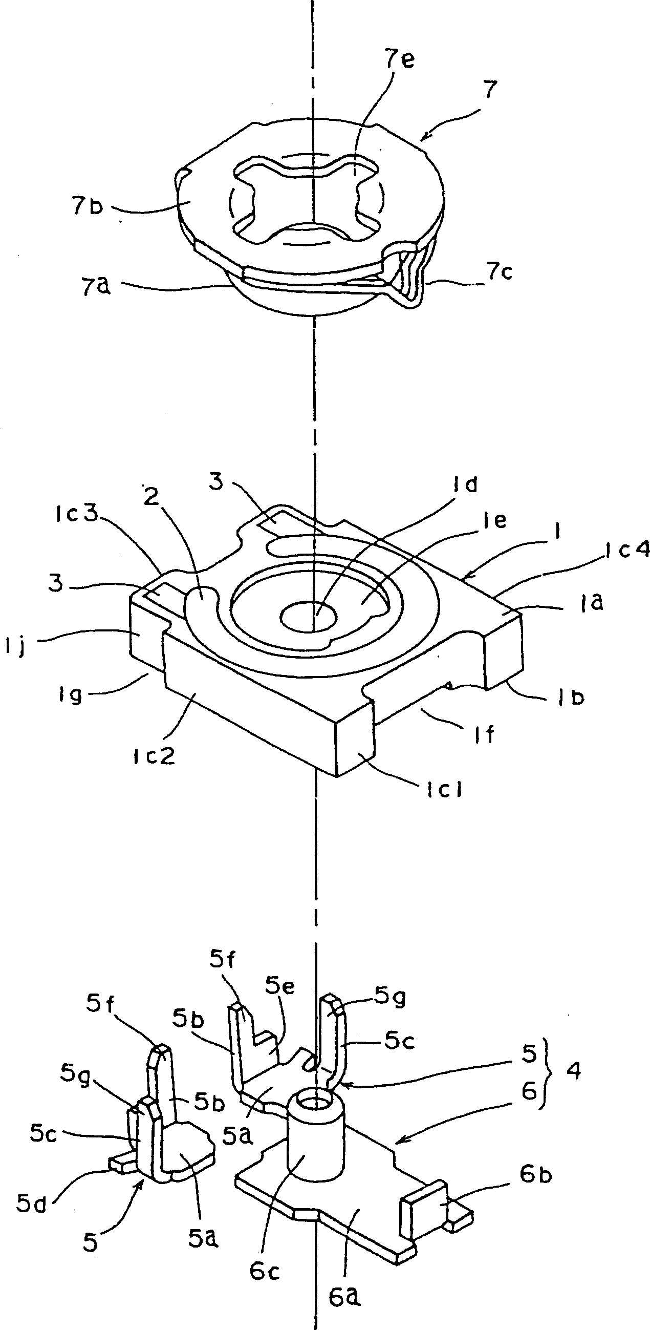
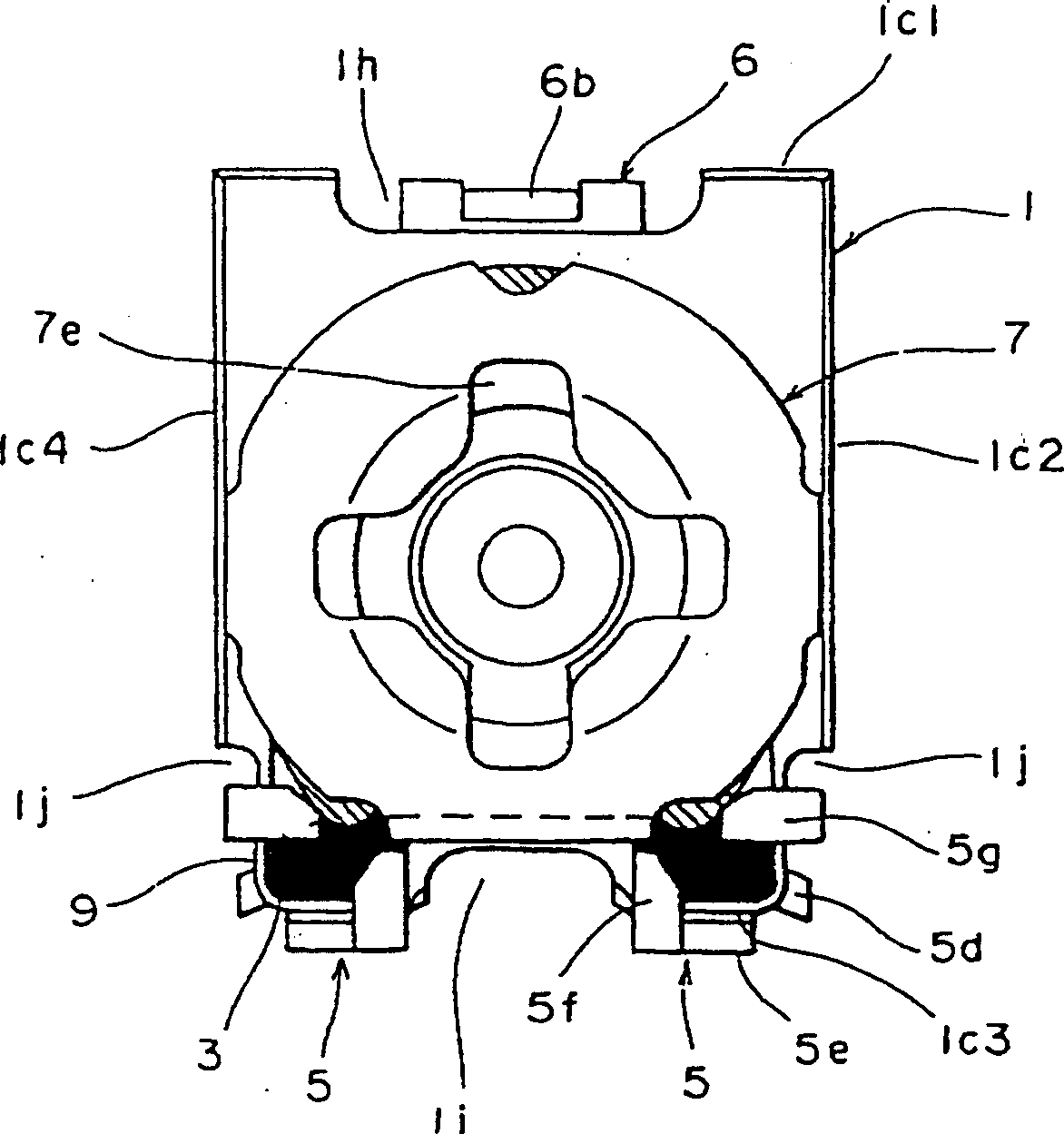
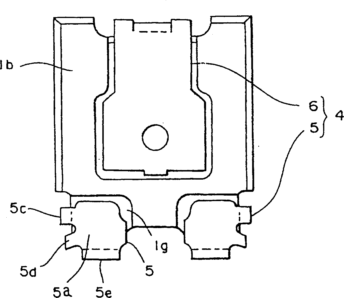
[0049] Such as Figure 1 to Figure 10 As shown, the insulating substrate 1 is made of ceramic material and is fired and processed into a slightly rectangular shape, and its length×width×thickness dimensions are about 3.5mm×3mm×0.8mm (volume about 8.4mm 3 ), has an upper surface 1a, a lower surface 1b, side surfaces 1c1 to 1c4 surrounding the circumference, and a circular hole 1d penetrating from the upper surface 1a to the lower surface 1b in the center. At the center of the upper surface 1a, there is provided a substantially circular recess 1e surrounding the hole 1d, and at the approximate center of the lower surface 1b, a rectangular shallow groove-like groove 1f is provided. The side surface 1c1 of one end of the groove 1f is directed Open to the outside.
[0050] On the opposite side 1c1 and side 1c3 ( figure 2 In the vertical direction), there are respectively a large width rectangular notch 1h and a narrow width rectangular notch 1i, and the opposite side surfaces 1c2 and 1c4 ( figure 2 In the left-right direction), a pair of rectangular cutout portions 1j sandwiching the electrode 3 and facing the aforementioned cutout portion 1i are provided.
[0051] On the bottom 1b, on the side of the aforementioned notch 1i (see image 3 ) Is provided with a pair of rectangular recesses 1g, which are recessed from the bottom 1b, and are connected to the two side surfaces 1c2 and 1c3, and side 1c3 and 1c4 that are orthogonally adjacent to each other, and their directions are formed toward State open to the outside. The depth dimension t2 of the recessed portion 1g and the groove portion 1f is approximately 0.2 mm, for example.
[0052] The above is the description of the way in which the orthogonally adjacent side faces 1c2 and 1c3 (and the side faces 1c3 and 1c4 directions) of the recess 1g are open, but it is not limited to this. It can also be made into three side faces that are open or facing each other. The shape of the two side openings.
[0053] The resistor 2 is made of, for example, a cermet paste or the like, and is formed in a substantially arc shape around the concave portion 1e of the upper surface 1a of the insulating substrate 1 by printing or the like.
[0054] The electrode 3 is made of, for example, a paste containing silver, has a substantially rectangular shape, is provided on the upper surface 1a of the insulating substrate 1, and is connected to both ends of the resistor 2 and formed as a pair by printing or the like. The electrode 3 is arranged in the vicinity of the corner formed by each of the side surfaces 1c2, 1c3 and the side surfaces 1c3, 1c4 of the insulating substrates 2 adjacent to each other.
[0055] The terminal 4 is made of a metal plate such as steel, copper, etc., and is formed by a pair of first terminal 5 and a second terminal 6 after punching and bending. The thickness (plate thickness) t3 of the terminal 4 is approximately 0.15 mm.
[0056] The first terminal 5 is equipped with a rectangular (quadrilateral) bottom plate 5a, a first leg part 5b and a second leg part 5c respectively bent upward from two adjacent side edges of the bottom plate 5a at right angles. A protruding portion 5d that protrudes outward from the bottom plate 5a between the portion 5b and the second leg portion 5c. One of the first leg portions 5b has a root portion 5e with a larger width and a tip portion 5f with a narrower width than the root portion 5e. The tip portion 5f extends upward from the root portion 5e and is bent slightly parallel to the bottom plate 5a. The width dimension of the other second leg portion 5c is formed from the root to the tip portion 5g to have the same width dimension and approximately the same width as the aforementioned tip portion 5f, and the tip portion 5g is bent slightly parallel to the bottom plate 5a.
[0057] The first terminal 5 is mounted on the insulating substrate 1. Specifically, the bottom plate 5a of the first terminal 5 is received in the recess 1g of the lower surface 1b of the insulating substrate 1, and the first leg 5b and the second The leg portion 5c is arranged along the two side surfaces 1c1, 1c3 and the side surfaces 1c3, 1c4 that are provided with the recessed portion 1g of the insulating substrate 1 and the corners are orthogonal to each other. The front end portions 5f of the first leg portion 5b and the second leg portion 5c, 5g is bent toward the upper surface 1a of the insulating substrate 1. In this state, the tip portions 5f, 5g of the first leg portion 5b and the second leg portion 5c are bent along the outer edge of the resistor 3 side of the electrode 3 provided on the upper surface 1a of the insulating substrate 1. The corners of the insulating substrate 1 are separated by a predetermined interval, so that a relatively large area not covered by the tip portions 5f and 5g is formed on the electrode 3.
[0058] The first leg portion 5b and the second leg portion 5c of the first terminal 5 are arranged in a state of being in contact with the orthogonal side surfaces 1c3, 1c4 and the side surfaces 1c2, 1c3. Thus, as described later, the substrate 1 is insulated during assembly. The positioning is easy.
[0059] In this state, the bottom plate 5a of the first terminal 5 in contact with the concave portion 1g of the insulating substrate 1 has a depth dimension t2 of approximately 0.2 mm, for example, and the thickness dimension (plate thickness) t3 of the bottom plate 5a is approximately 0.15 mm, for example. Therefore, a gap t1 (t1=t2-t3) of about 0.05 mm is formed between the lower surface 1b of the insulating substrate 1 and the lower surface of the bottom plate 5a. That is, the bottom plate 5a of the first terminal 5 is arranged in a state of being housed in the recess 1g of the insulating substrate 1.
[0060] The inventors conducted various experiments on the gap t1, and as a result, it was proved that the gap t1 should be within the range of 0
[0061] The second terminal 6 is equipped with a slightly rectangular bottom plate 6a, a cut-and-raised portion 6b punched upward on one end of the bottom plate 6a, and a cylindrical hollow shaft portion deep drawn upward on the other end of the bottom plate 6a. 6c.
[0062] The second terminal 6 is mounted on the insulating substrate 1. Specifically, the bottom plate 6a of the second terminal 6 is accommodated in the groove 1f of the lower surface 1b of the insulating substrate 1, and abuts it, and the hollow shaft portion 6c penetrates the insulating substrate 1. The cut-and-raised portion 6b of the hole 1d extends along the inner wall of the notch 1h provided on the side surface 1c1 of the insulating substrate 1 in the direction of the upper surface 1a.
[0063] In this state, similarly to the aforementioned first terminal 5, a gap of approximately 0.05 mm is formed between the lower surface 1b of the insulating substrate 1 and the lower surface of the second terminal 6.
[0064] The slider 7 is made of a metal plate such as stainless steel, copper or its alloy, and is processed as a whole by punching and bending, and has a holding portion 7a that is formed into a substantially disc shape by deep drawing and is arranged above the holding portion 7a. Section 7b, a U-shaped sliding section 7c extending from the holding section 7a. In the center of the holding portion 7a, a circular hole 7d is formed (see Figure 4 ), a cross-shaped hole 7e is formed in the center of the operation portion 7b.
[0065] The holding portion 7a of the slider 7 is arranged in the recess 1e of the upper surface 1a of the insulating substrate 1, the hollow shaft portion 6c of the second terminal 6 is in a state of penetrating the hole 1d of the insulating substrate 1, and the tip portion of the hollow shaft portion 6c penetrates The hole 1d is squeezed into the hole 7d of the holding portion 7a. In this state, the slider 7 can rotate relative to the insulating substrate 1. At this time, the slider 7 is in contact with the second terminal 6.
[0066] At this time, the sliding portion 7c of the slider 7 is in elastic contact with the resistor 2 provided on the upper surface 1a of the insulating substrate 1, and the sliding portion 7c slides on the resistor 2 in response to the rotation of the slider 7.
[0067] The solder 9 is a solder with a higher melting point than solder with a general melting point (for example, about 180 degrees), and its melting point is in the temperature range of 220 degrees to 330 degrees. The soldering 9 connects the electrode 3 provided on the upper surface 1a of the insulating substrate 1, the tip portion 5f of the first leg portion 5b of the first terminal 5, and the tip portion 5g of the second leg portion 5c. At this time, a relatively large area not covered by the tip 5f and the tip 5g of the electrode 3 becomes a solder zone, and the electrode 3 is soldered to the tip 5f and the tip 5g of the solder zone. The reason why the melting point temperature range of the solder 9 is between 220°C and 330°C is that if the melting point is too low, it needs to be re-melted during installation, which is troublesome. If the melting point is too high, a lot of heat is required for soldering. This heat has an adverse effect on the surrounding structural components, so it is set in the aforementioned temperature range.
[0068] Next, the method of manufacturing the chip variable resistor according to the embodiment of the present invention will be described.
[0069] Figure 13A , Figure 13B , Figure 13C , Figure 13D It is a process drawing explaining the manufacturing method of the chip varistor of this invention. As shown in the figure, first in the initial Figure 13A In the process, the terminal ferrule 10 is deep-drawn to form a cylindrical hollow shaft portion 6c, and at the same time the guide hole 11 is formed.
[0070] Then on the terminal hoop 10, a frame portion 12 is formed at a predetermined interval, and a pair of first terminals 5 and a second terminal 6 are formed. At this time, the cut-and-raised portions 6b of the second terminal 6 are simultaneously punched, and a pair of first The first leg 5b and the second leg 5c of the one terminal 5 are respectively bent upward from both side edges of the bottom plate 5a.
[0071] Hereinafter, the terminal hoop formed by the deep drawing, bending, and cutting steps will be described in detail.
[0072] Picture 11 A plan view showing the main part of the terminal ferrule in the terminal manufacturing process of the chip varistor according to the embodiment of the present invention. Picture 12 Is along Picture 11 Sectional view of line 12-12.
[0073] Such as Picture 11 , Picture 12 As shown, the terminal hoop 10 is made of a strip metal plate such as steel, copper, etc., and is formed through deep drawing, punching, bending, and cutting processes. The terminal hoop 10 has a plurality of substantially rectangular frame portions 12 formed continuously, and guide holes 11 provided at predetermined intervals opposite to the plate width direction of the frame portion 12.
[0074] The frame portion 12 is provided with a pair of protruding portions 5d, a substantially quadrangular bottom plate 5a (first terminal 5), and a second terminal 6. The pair of protrusions 5 d protrude inward of the frame 12 from the vicinity of the guide hole 11 and are connected to the frame 12. The bottom plate 5a is connected to each protrusion 5d. The second terminal 6 protrudes inward of the frame portion 12 from between two adjacent guide holes 11 and is connected to the frame portion 12. The bottom plate 5a is formed with a first leg 5b and a second leg 5c that are bent upward with the protrusion 5d interposed therebetween.
[0075] Such as Figure 13B As shown, in the placement and densification process, a semi-finished product composed of an insulating substrate 1 on which resistors 2 and electrodes 3 are provided, manufactured in another process (not shown), is placed on the terminal ring 10 The frame portion 12 is connected to the bottom plate 5a of the first terminal 5 and the second terminal 6. At this time, the side surfaces 1c3, 1c2 (and side surfaces 1c3, 1c4) of the semi-finished insulating substrate 1 are connected to the first leg 5b and the second leg 5c of the first terminal 5, and the insulating substrate 1 is connected to the terminal hoop. 10. Positioning.
[0076] At this time, the hollow shaft portion 6c of the second terminal 6 penetrates the hole 1d of the insulating substrate 1.
[0077] After this placement process, the front ends 5f and 5g of the first leg 5b and the second leg 5c are bent toward the upper surface 1a of the insulating substrate 1, and the first terminal 5 and the second terminal 6 are crimped Bending process on semi-finished products. In this bending step, the tip portions 5f and 5g of the first leg portion 5b and the second leg portion 5c are bent along the outer edge near the boundary of the resistor body 2 of the electrode 3, and the electrode 3 is provided with a relatively large Soldering area.
[0078] Then, in Figure 13C In the soldering process, the first leg portion 5b of the first terminal 5 and the tip portions 5f, 5g of the second leg portion 5c are soldered to the soldering area provided on the electrode 3 by high-temperature soldering, and the first terminal is connected to the electrode 3 .
[0079] Next, in the slider assembly and cutting process, the slider 7 is assembled on the semi-finished product to which the first terminal 5 is soldered, and the assembled slider 7 is crimped on the hollow shaft portion 6c of the second terminal 6, the semi-finished product and The slider 7 and the second terminal 6 are integrated into Figure 13D In the single product cutting process, the vicinity of the cut-and-raised portion 6b of the second terminal 6 and the protruding portion 5d of the first terminal 5 are cut, and the chip varistor as a single product is separated from the frame body 11.
[0080] Next, a method of mounting the chip variable resistor of the embodiment of the present invention on a printed circuit board will be described.
[0081] Figure 14 It is a cross-sectional view showing a state where the chip varistor of the embodiment of the present invention is mounted on a printed circuit board.
[0082] Such as Figure 14 As shown, the printed circuit board 20 is composed of, for example, a synthetic resin material added with glass, and is formed in a flat plate shape. On at least one surface of the printed circuit board 20, a desired conductive pattern (not shown) is formed. The above-mentioned chip varistor of the present invention is placed on the conductive pattern (not shown) of the printed circuit board 20. At this time, the solder paste 13 is applied to a predetermined conductive pattern, and the first terminal 5 and the second terminal 6 of the chip varistor are placed and connected to the solder paste 13.
[0083] The melting point of the solder paste 13 is, for example, 180 degrees, which is lower than the melting point (220 degrees to 330 degrees) of the first terminal 5 soldered to the electrode 3.
[0084] In this state, the printed circuit board 20 on which the chip varistor is placed is placed in a reverberatory furnace (not shown, the temperature in the reverberatory furnace is about 220 degrees), and the chip varistor and the printed circuit The conductive pattern 21 of the substrate 20 is connected by soldering, and if the temperature of the reverberatory furnace is set to a high temperature not higher than the melting point of the solder by 40 to 50 degrees, the solder cannot melt, which is well known. The first terminal 5 and the electrode 3 of the chip varistor are connected by high-temperature soldering. The temperature in the reverberatory furnace is set to be about 40-50 degrees higher than the melting point of the solder paste 13. Therefore, the reverberatory furnace The temperature of the solder paste 13 melts, and at the same time, the high temperature solder does not melt, which can realize a stable solder connection.
[0085] At this time, gaps are formed between the lower surface of the insulating substrate 1 of the chip varistor and the lower surface of the bottom surface 5a of the first terminal 5, and between the lower surface of the insulating substrate 1 and the lower surface of the second terminal 6, respectively, Since the recessed portion 1g and groove portion 1f of the insulating substrate 1 are open in the side surface direction, when the first and second terminals 5 and 6 of the chip varistor are soldered to the printed circuit board 20, the soldering The flux and solvent in the paste can be scattered from the open part in the side direction through the aforementioned gap.
[0086] In the foregoing embodiment, the bottom plate 5a of the first terminal 5 is arranged in the recess 1g of the insulating substrate 1, and a gap t1 is provided between the bottom surface 1b of the insulating substrate 1 and the bottom plate 5a. However, it is also possible to arrange the bottom plate 5a of the first terminal 5 in the recess 1g of the insulating substrate 1 so that the bottom surface 1b of the insulating substrate 1 is flush with the bottom plate 5a of the first terminal 5 without the aforementioned gap t1, or Slightly flush. In this way, it is possible to achieve a thin profile and at the same time achieve a stable placement state during installation.
[0087] Similarly for the second terminal 6, the bottom plate 6a of the second terminal 6 can be arranged in the recess 1g of the insulating substrate 1, so that the bottom surface 1b of the insulating substrate 1 is flush with or slightly flush with the bottom plate 6a of the second terminal 6. It is thinner and can be placed in a stable state during installation.
[0088] As described above, the chip varistor of the present invention is provided with at least two recessed portions open in the lateral direction on the underside of the insulating substrate, and the bottom plate of the first terminal is arranged in the recessed portion of the insulating substrate. Therefore, the ceramic substrate can be prevented from Cracking, thinning can be achieved, and a stable placement state during installation can be achieved.
[0089] In the chip varistor of the present invention, the recesses of the insulating substrate are formed at the corners of the insulating substrate, and the adjacent side surfaces are open at right angles to each other. Therefore, the insulating substrate has a simple structure and can provide an inexpensive chip varistor .
[0090] In the chip varistor of the present invention, the bottom plate of the first terminal is arranged in the recesses of the insulating substrate opened in at least two side directions, and a gap is formed between the bottom surface of the insulating substrate and the bottom surface of the bottom plate. When the solder paste electrically and mechanically connects the chip varistor to the printed circuit board, when the solvent contained in the solder paste volatilizes, the volatilized solvent can pass through the gap and move from at least two side surfaces of the recess The open part is discharged to the outside of the chip variable resistor. Therefore, the contact and connection of the soldered part can be reliably performed, and poor conduction can be avoided.
[0091] In the chip varistor of the present invention, since the gap t1 between the bottom surface of the insulating substrate and the bottom surface of the bottom plate is 0
[0092] In addition, in the chip varistor of the present invention, the second terminal is accommodated in the groove, and a gap is formed between the underside of the insulating substrate and the underside of the second terminal. Therefore, the second terminal can be reliably accommodated in the groove. , The solvent volatilized when the chip varistor is electrically and mechanically connected to the printed circuit board with solder paste can be discharged to the outside of the chip varistor through the gap. Therefore, the contact and connection of the soldered part can be reliably performed, and poor conduction can be avoided.

PUM

no PUM

Description & Claims & Application Information

We can also present the details of the Description, Claims and Application information to help users get a comprehensive understanding of the technical details of the patent, such as background art, summary of invention, brief description of drawings, description of embodiments, and other original content. On the other hand, users can also determine the specific scope of protection of the technology through the list of claims; as well as understand the changes in the life cycle of the technology with the presentation of the patent timeline. Login to view more.
Why Eureka
Try Eureka