Method for producing electronic component
A technology of electronic components and resistors, applied in nanotechnology for sensing, manufacturing resistors through photolithography, resistor manufacturing, etc., can solve problems such as poor yields
Pending Publication Date: 2022-06-21
INFINEON TECH AG
View PDF0 Cites 0 Cited by
- Summary
- Abstract
- Description
- Claims
- Application Information
AI Technical Summary
Problems solved by technology
This leads to poor yields in subsequent d
Method used
View moreImage
Smart ImageViewing Examples

Examples
 PUM
 Abstract
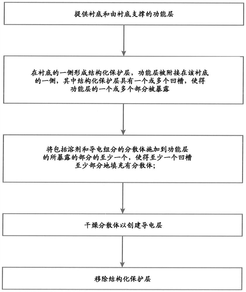
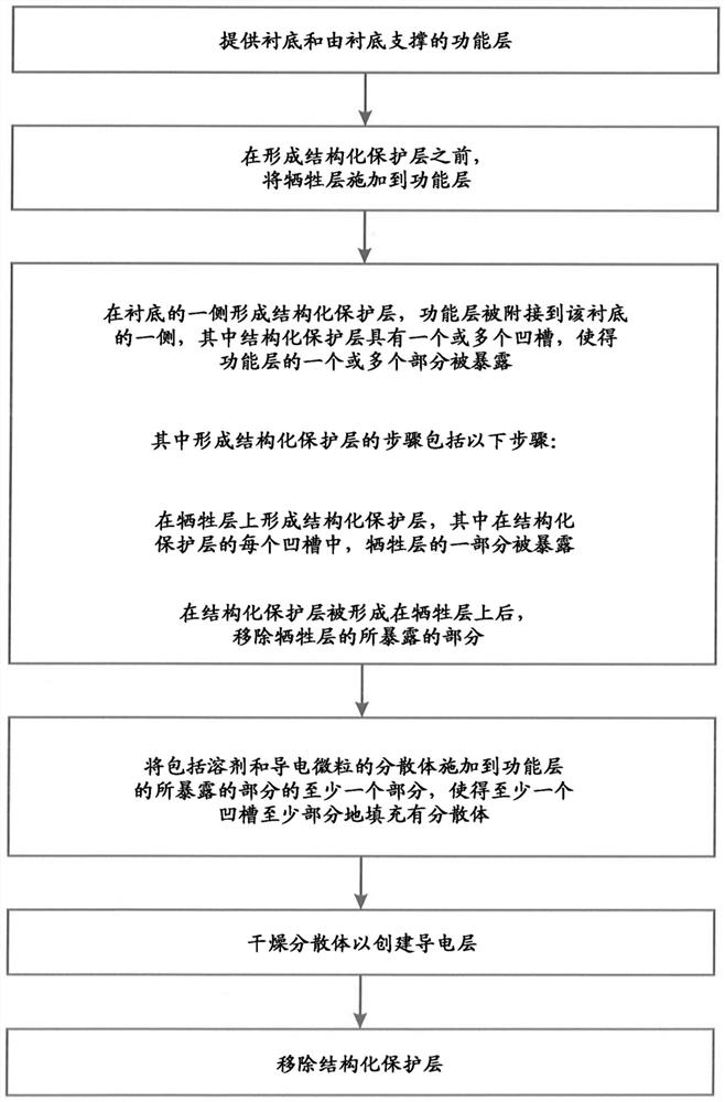
Embodiments of the present disclosure relate to a method for manufacturing an electronic component wherein the method comprises the steps of: providing a substrate and a functional layer supported by the substrate; forming a structured protective layer on one side of the substrate, the functional layer being attached to one side of the substrate, where the structured protective layer has a recess such that a portion of the functional layer is exposed; applying a dispersion comprising a solvent and a conductive component to the exposed portion of the functional layer such that the recess is at least partially filled with the dispersion; drying the dispersion to create a conductive layer; and removing the structured protection layer.
Description
technical field [0001] Embodiments relate to a method for manufacturing an electronic component. More specifically, embodiments relate to a method for manufacturing an electronic component, wherein a dispersion is applied to a functional layer and dried to create a conductive layer. Background technique [0002] Obtaining a conductive layer with a defined pattern by applying and drying the dispersion is a challenge when using selective deposition techniques such as inkjet printing. In particular, the accumulation of material on the edges of the pattern of the conductive layer due to the Marangoni effect results in conductive paths surrounding the desired pattern of the conductive layer. This results in poor yields in subsequent devices such as chemi-resistive gas sensors. [0003] Therefore, there is a need for an improved method for manufacturing electronic components. SUMMARY OF THE INVENTION [0004] This problem is solved by a method for manufacturing electronic com...
Claims
Login to view more Application Information
Patent Timeline
 IPC IPC(8): G01N27/12
CPCG01N27/12G01N27/128G01N27/22B82Y15/00G01N27/125G01N27/129G01N27/123C23C16/26C23C16/56H01C17/003H01C17/06506
Inventor M·迈耶J·E·阿达蒂·埃斯特维兹A·M·罗斯
Owner INFINEON TECH AG
- R&D Engineer
- R&D Manager
- IP Professional
Why Eureka
- Industry Leading Data Capabilities
- Powerful AI technology
- Patent DNA Extraction
Try Eureka
Browse by: Latest US Patents, China's latest patents, Technical Efficacy Thesaurus, Application Domain, Technology Topic.
© 2024 PatSnap. All rights reserved.Legal|Privacy policy|Modern Slavery Act Transparency Statement|Sitemap