Supercharge Your Innovation With Domain-Expert AI Agents!

Pattern etching agent of In-Sn oxide and LCD making process

An indium tin oxide, etchant technology, applied in chemical instruments and methods, semiconductor/solid-state device manufacturing, transistors, etc., can solve problems such as degradation of liquid crystal display devices

Inactive Publication Date: 2006-08-09
LG DISPLAY CO LTD
View PDF0 Cites 0 Cited by
  • Summary
  • Abstract
  • Description
  • Claims
  • Application Information

AI Technical Summary

Problems solved by technology

As a result, the liquid crystal display device will be degraded

Method used


Image

  • Pattern etching agent of In-Sn oxide and LCD making process
  • Pattern etching agent of In-Sn oxide and LCD making process
  • Pattern etching agent of In-Sn oxide and LCD making process

Examples


Embodiment Construction

[0040] Embodiments of the present invention will be described in detail below with reference to examples illustrated in the accompanying drawings. Wherever possible, the same reference numbers will be used throughout the drawings to refer to the same or like parts.

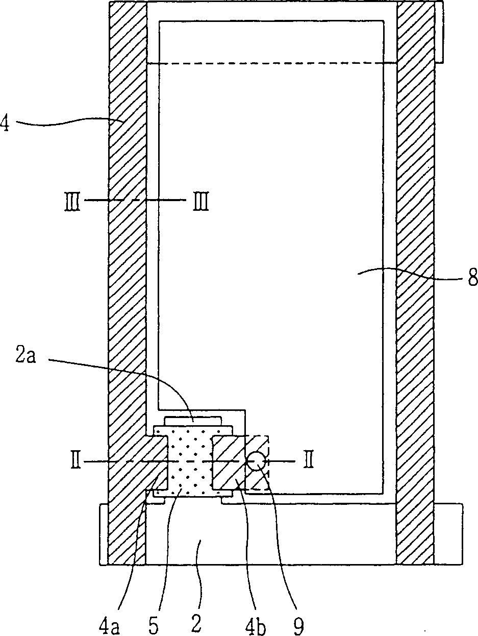
[0041] Figures 4A to 4D is a diagram illustrating the process by using the ITO etchant according to the present invention along the figure 1 Sequential sectional view of line II-II;

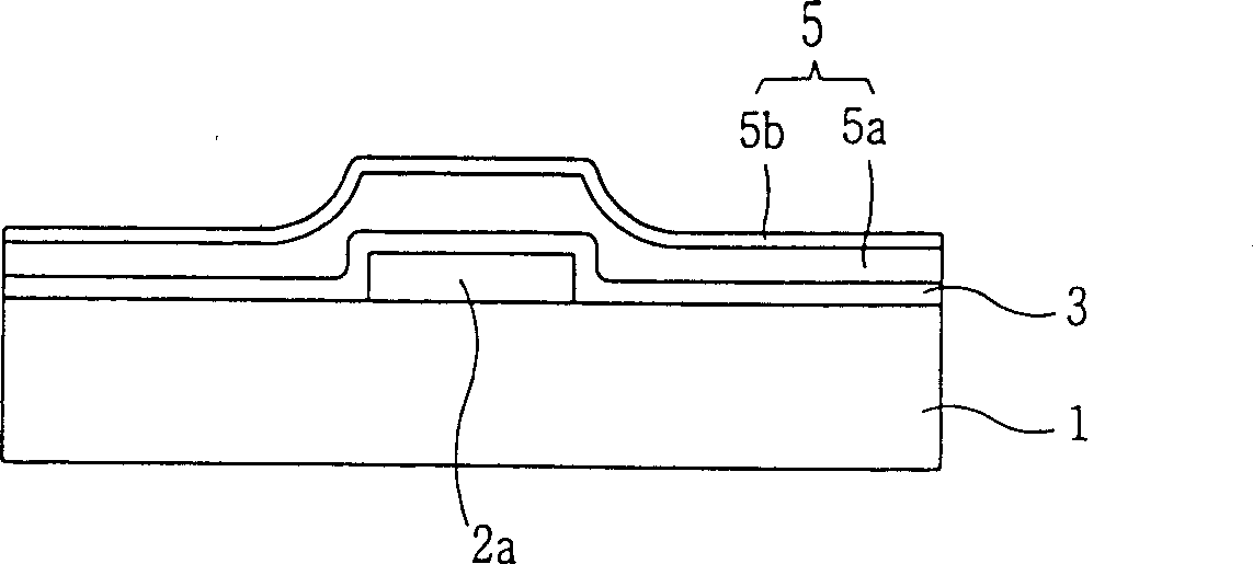
[0042] Such as Figure 4A A gate electrode 2a is formed on a glass substrate 1 as shown. On the gate electrode 2a including the substrate 1, the gate insulating film 3, amorphous silicon 5a and n + Amorphous silicon 5b.

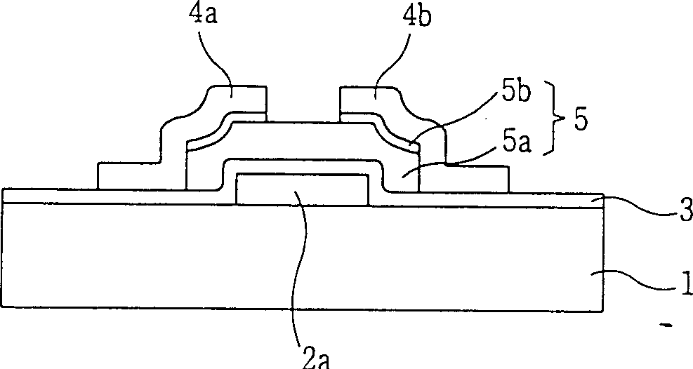
[0043] exist Figure 4B , by patterning amorphous silicon 5a and n + Amorphous silicon 5 b forms the active region 5 . The source electrode 4a and the drain electrode 4b are formed separately from each other on the active region 5 (including the side surface of the active region 5). Mo or Mo alloy is depos...


PUM


Abstract

An etchant for patterning indium tin oxide, wherein the etchant is a mixed solution of HCl, CH3COOH, and water, and a method of fabricating a liquid crystal display device are disclosed in the present invention. The method includes forming a gate electrode on a substrate, forming a gate insulating layer and an amorphous silicon layer on the gate electrode including the substrate, forming an active area by patterning the amorphous silicon layer, forming a source electrode and a drain electrode on the active area, forming a passivation layer on the source electrode and the drain electrode and the gate insulating layer, forming a contact hole exposing a part of the drain electrode, forming an indium tin oxide layer on the passivation layer, and forming an indium tin oxide electrode by selectively etching the indium tin oxide layer using a mixed solution of HCl, CH3COOH, and water as an etchant.

Description

technical field [0001] The invention relates to an etchant, in particular to an etchant for patterning indium tin oxide. Although the present invention is suitable for a wide range of applications, it is more suitable for preventing damage and precipitation of the bottom layer during the etching process. Background technique [0002] Typically, HCl and HNO are used 3 mixed solution or oxalic acid (C 2 h 2 o 4 ), etch the indium tin oxide (ITO) used as the transparent electrode of the display device to form a pattern. Hereinafter, an etching process of amorphous ITO (a-ITO) used to manufacture a thin film transistor display device will be described with reference to the accompanying drawings. [0003] figure 1 is a plan view showing one unit pixel of the thin film transistor display device. As shown, the gate line 2 and the data line 4 are arranged to cross each other. A pixel electrode 8 formed of a transparent metal such as ITO is disposed in a pixel area defined by...

Claims


Application Information

Patent Timeline
Patent Type & Authority Patents(China)
IPC IPC(8): G02F1/136H01L21/00C09K13/06G02F1/1343G02F1/1368H01L21/308H01L21/336H01L21/77H01L21/84H01L27/12H01L29/786H01L31/18
CPCH01L27/1214H01L27/124Y02E10/50H01L31/1884G02F1/13439C09K13/06G02F1/136
Inventor 卢柄兑安维新
Owner LG DISPLAY CO LTD
Features
  • R&D
  • Intellectual Property
  • Life Sciences
  • Materials
  • Tech Scout
  • Unparalleled Data Quality
  • Higher Quality Content
  • 60% Fewer Hallucinations
Learn More