

Latching effect detecting method for CMOS circuit
A test method and technology of latch-up effect, applied in the field of testing, can solve the problems of complex trigger source pulse waveform and inconvenient actual use, and achieve the effect of reducing design cost and use risk, and simple pulse waveform
- Summary
- Abstract
- Description
- Claims
- Application Information
AI Technical Summary
Problems solved by technology
Method used
Image

Examples
Embodiment Construction
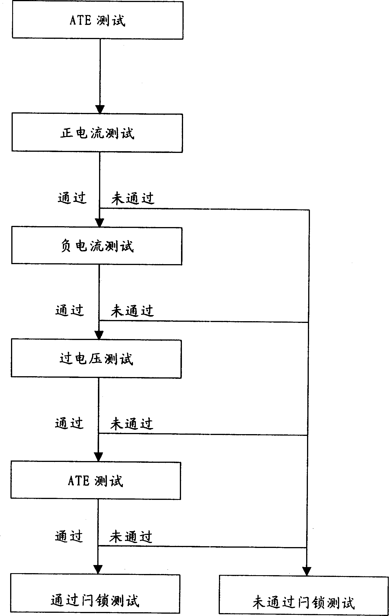
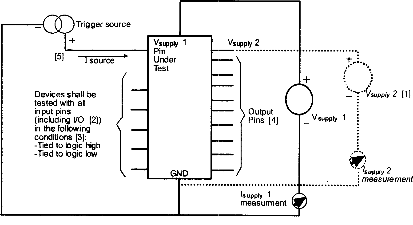
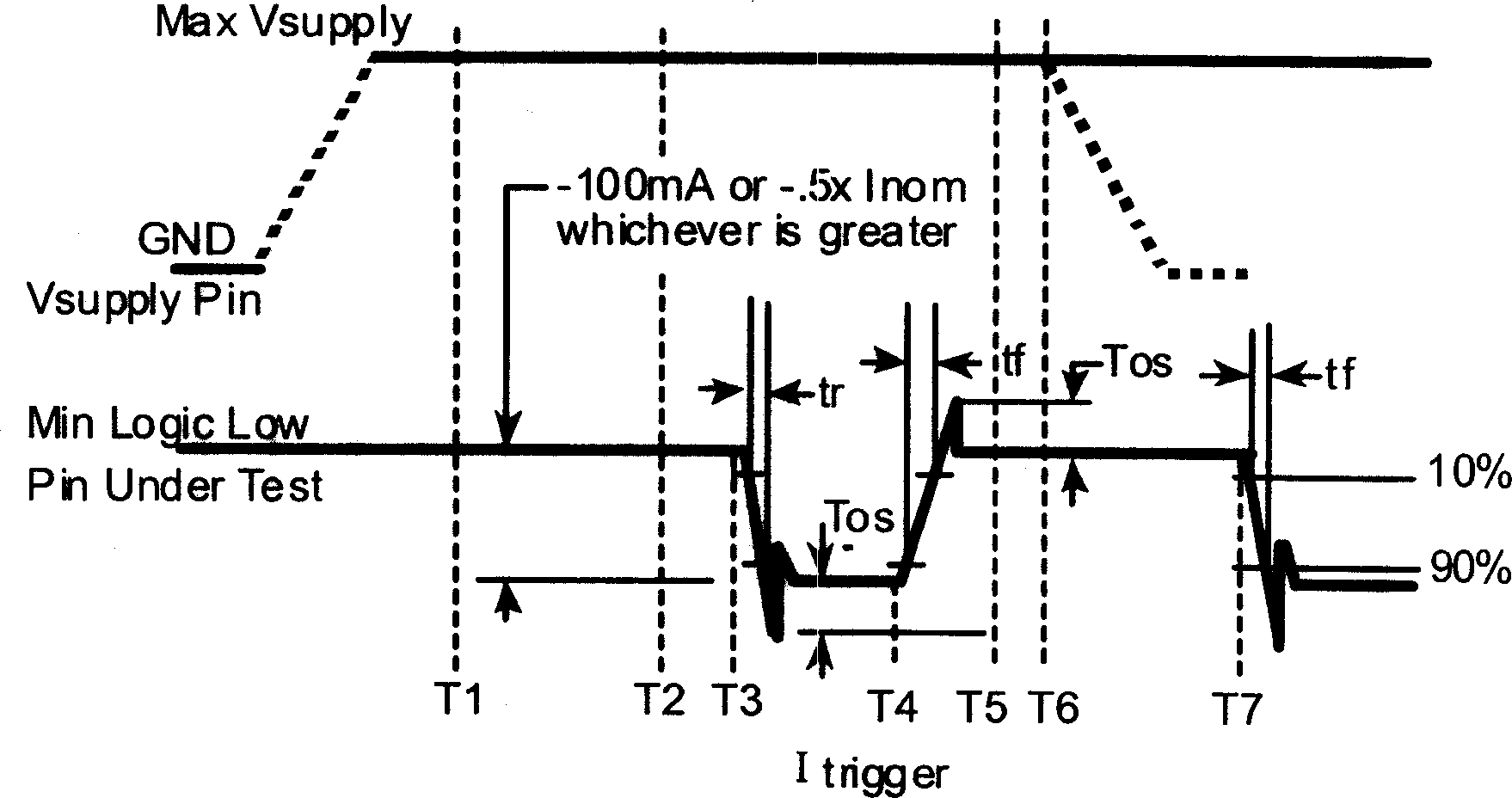
[0032] see Figure 8 As shown, the latch-up test method of the CMOS circuit of the present invention can be used for testing the trigger voltage / current of the CMOS integrated circuit, the accurate value of the maintenance voltage / current and the secondary breakdown voltage / current anti-latch-up ability parameter, firstly during the test Connect all the input terminals of the device under test to the ground, and the output terminals are suspended, and then proceed as follows:
[0033] Step 1: First, perform a DC voltage scanning test on the terminal to be tested until the terminal to be tested conducts to the ground, and obtain the trigger voltage Von of the terminal to be tested. During specific implementation, the scanning range of the DC voltage can start from 0V, the step size is 0.5V, and the current limit is 50mA. It can be seen from the IV characteristics of the power supply terminal that the current is very small when the voltage is less than a certain value, and the ...
PUM
 Abstract
Description
Claims
Application Information