Substrate holding device and polishing device

A substrate holding and substrate technology, which is applied in the directions of grinding devices, electrical components, circuits, etc., can solve the problem that the grinding rate of semiconductor wafers cannot be fully and arbitrarily controlled.

Inactive Publication Date: 2005-11-16
EBARA CORP
View PDF0 Cites 19 Cited by
  • Summary
  • Abstract
  • Description
  • Claims
  • Application Information

AI Technical Summary

Problems solved by technology

In the existing polishing apparatus, the current situation is that the polishing rate of the...

Method used


Image

  • Substrate holding device and polishing device
  • Substrate holding device and polishing device
  • Substrate holding device and polishing device

Examples


Embodiment approach

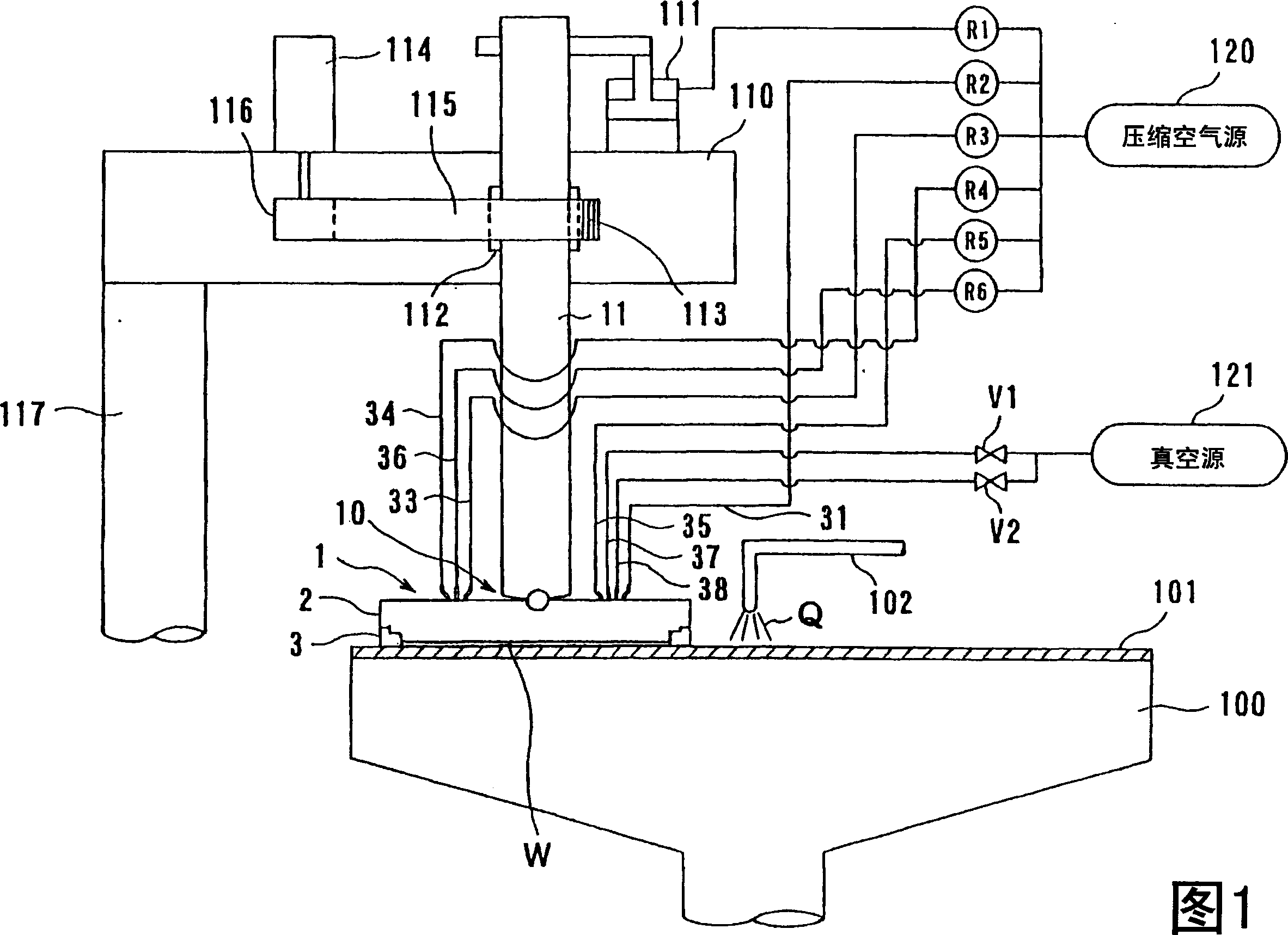
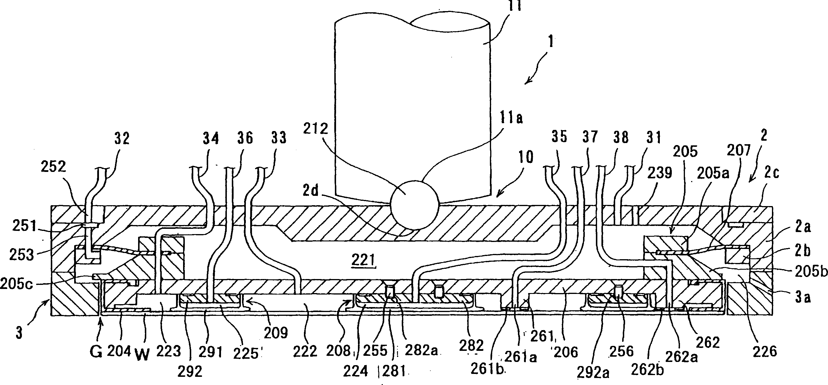
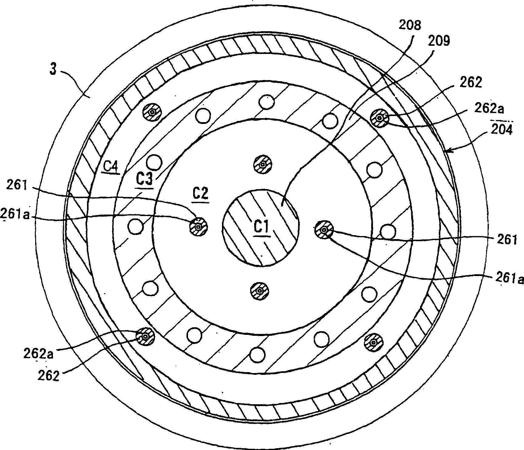
[0070] FIG. 1 is a cross-sectional view showing the overall structure of a polishing apparatus including a substrate holding device according to the present invention. Here, the substrate holding device is a device that holds a substrate such as a semiconductor wafer as an object to be polished and presses it against a polishing surface on a polishing table. As shown in FIG. 1 , below a top ring 1 constituting a substrate holding device according to the present invention, a polishing table 100 on which a polishing pad 101 is pasted is provided. In addition, a polishing liquid supply nozzle 102 is provided above the polishing table 100 , and the polishing liquid Q is supplied to the polishing pad 101 on the polishing table 100 through the polishing liquid supply nozzle 102 .

[0071] In addition, as a commercially available polishing pad, there are various pads, for example, SUBA800, IC-1000, IC-1000 / SUBA400 (two-layer cloth) manufactured by Rodell Corporation, Fujimi Co., Ltd....


PUM

PropertyMeasurementUnit
Radial lengthaaaaaaaaaa

Abstract

The present invention relates to a substrate holding apparatus for holding a substrate (W) such as a semiconductor wafer in a polishing apparatus for polishing the substrate to a flat finish. A substrate holding apparatus according to the present invention comprises a top ring body (2) having a receiving space therein, and a vertically movable member (206) which is vertically movable within the receiving space in the top ring body. An abutment member (209) having an elastic membrane is attached to a lower surface of the vertically movable member. The elastic membrane (291) of the abutment member comprises an abutment portion (291b), having a flange (291a) projecting outwardly, brought into direct or indirect contact with the substrate, and a connecting portion (291c) extending upwardly from a base portion (291d) of the flange of the abutment portion and being connected to the vertically movable member. The connecting portion is made of a material having a flexibility higher than the abutment portion.

Description

technical field [0001] The present invention relates to a substrate holding device that holds a substrate to be polished and presses it against a polishing surface, and more particularly relates to a polishing device that holds a substrate such as a semiconductor wafer and then planarizes it. Substrate holding device for substrates. In addition, the present invention relates to a polishing apparatus provided with such a substrate holding device. Background technique [0002] In recent years, semiconductor devices have become more miniaturized and their device structures have become more complex. In addition, as the number of layers of logic multilayer wiring increases, the surface irregularities of semiconductor devices also increase, and the level difference tends to increase. This is because in the manufacture of semiconductor devices, the process of forming a thin film and forming the next thin film after performing microfabrication of patterning or opening is repeated m...

Claims


Application Information

Patent Timeline
IPC IPC(8): B24B37/005B24B37/30H01L21/304H01L21/68H01L21/683
Inventor 户川哲二锅谷治福岛诚樱井邦彦吉田博市村照彦
Owner EBARA CORP
Why Eureka
Try Eureka