Signaling with multiple clock lines

A signal and reference time technology, applied in the direction of synchronous information channel, line failure/interference reduction, digital transmission system, etc., can solve problems such as high cost, cost of increasing power and circuit board wiring space, limiting channel throughput, etc.

Inactive Publication Date: 2006-09-13
INTEL CORP
View PDF2 Cites 2 Cited by
  • Summary
  • Abstract
  • Description
  • Claims
  • Application Information

AI Technical Summary

Problems solved by technology

Moreover, interactions between residual signal components output by previous symbols contribute to intersymbol interference (ISI), which further limits channel throughput
These impairments in physical channel capacity can be mitigated somewhat by using higher performance components and board materials, but this incurs a greater cost
Adding additional data lines to the bus also increases costs in terms of power and board layout space

Method used


Image

  • Signaling with multiple clock lines
  • Signaling with multiple clock lines
  • Signaling with multiple clock lines

Examples


Embodiment Construction

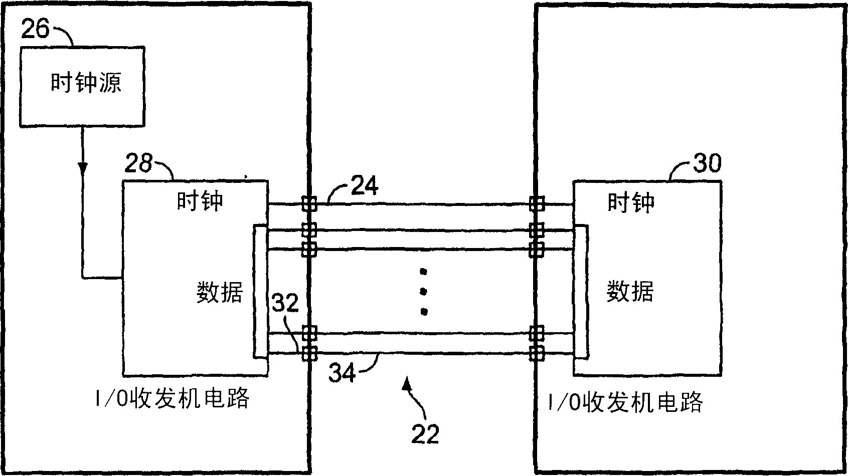
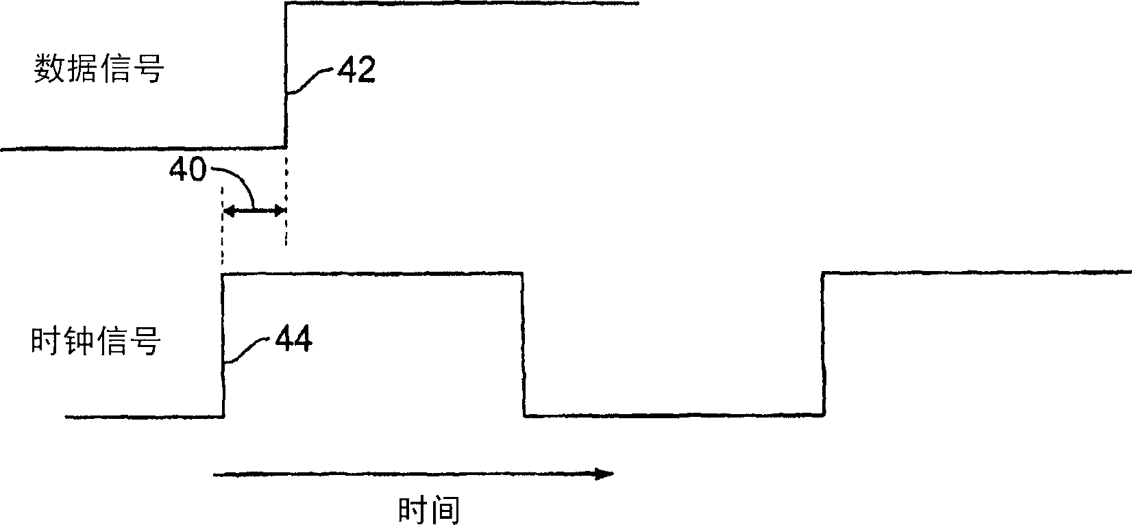
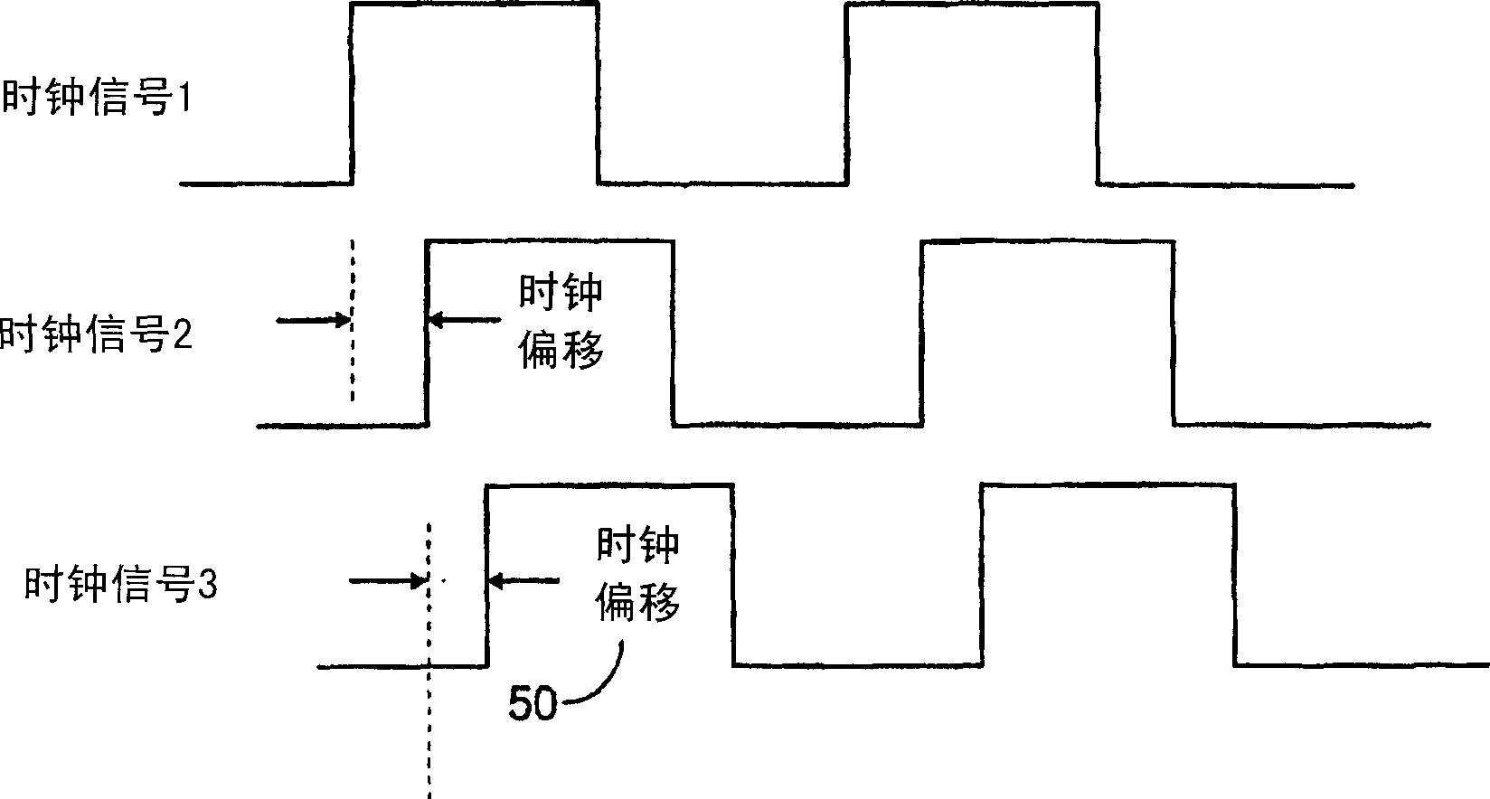
[0028] Multiple time reference signals (clocks) can be used to improve the timing resolution of eg phase and pulse width modulated signals. Such as image 3 As shown, clock signals can be derived from the same source, but the clock signals are phase shifted with respect to each other by a pre-designed amount 50. The modulator circuit can then reference the data transition to the clock signal whose edge is closest to the transition. Because there are more clock transitions, the time interval from a data signal transition to the nearest clock transition can be reduced. The integral of jitter, which increases with the event distance between a data transition and its reference clock transition, will also decrease, resulting in an overall reduction in circuit jitter. This results in a higher available bandwidth. In some embodiments, the addition of more than one clock signal may require sacrificing a considerable data line for each additional clock signal due to wire routing con...


PUM


Abstract

At least two sequences of predetermined reference times are established on respective ones of at least two communication lines. At least some of the reference times of at least one of the sequences occur out-of-phase with at least some of the reference times of another of the sequences. Digital data is encoded onto data signals on one or more communication lines such that a time difference between at least one of the data signals and the nearest one of the reference times on one of the communication lines is smaller than the time difference between the same data signal and the nearest one of the reference times on another one of the communication lines.

Description

technical field [0001] The present invention relates to signaling with multiple clocks. Background technique [0002] Signaling between active devices or integrated circuits (ICs) mounted on a computer circuit board typically relies on a combination of plug-ins, sockets, connectors, cables, and printed circuit board features to achieve the physical interconnection. refer to figure 1 , such chip-to-chip communication is often implemented as many parallel data interconnects comprising bus 22 . In some signaling modes, digital data is represented as pulse timing carried on each interconnect with respect to one or more clock signals carried on clock line 24 provided by common source 26 . Forward clock signals are generally routed in a manner similar to their accompanying data signals. Signals between input / output (I / O) transceivers 28 and 30 must traverse channel segment 32 on IC 32 and channel segment 34 between the ICs, which are impaired and are not practical for low cost ...

Claims


Application Information

Patent Timeline
Patent Type & Authority Applications(China)
IPC IPC(8): H04L7/00H04L25/493H04L25/08
CPCH04L25/493H04L7/0008H04L25/085H04L7/00H04L25/08H04L7/02
Inventor L·塔特T·威格
Owner INTEL CORP
Why Eureka
Try Eureka