Physical value sensor and lead frame for use therein

A technology of physical quantity sensor and lead frame, applied in the field of lead frame

Inactive Publication Date: 2007-06-06
YAMAHA CORP
3 Cites 2 Cited by

AI-Extracted Technical Summary

Problems solved by technology

[0008] However, in the conventional physical quantity sensor, in order to arrange the physical quantity sensor chip on the inclined installation surface, the packag...

Method used

[0111] Above the protruding pieces 19 and 21, a metal mold F having a flat surface F1 is provided, and clamps the rectangular frame portion 13 of the lead frame 1 together with the metal mold E described above. Between the lead frame 1 and the mold F, a thin plate S is inserted to prevent resin burrs adhering to the lead 15 and to facilitate peeling of the mold F and the resin.
[0126] In the lead frame 1 and the magnetic sensor 30 described above, the easy-to-deform part for inclining the table parts 7 and 9 is formed in the midway part 17d of the connecting wire 17. Therefore, the front-end|tip part 17a of the connection lead wire 17 which is closer to the stage part 7,9 side than this easy-to-deform part is inclined together with the stage part 7,9. Therefore, when the magnetic sensor chips 3 and 5 are arranged and tilted on the tip portion 17a, the magnetic sensor chips 3 and 5 and the connecting wire 17 do not interfere with each other (contact). That is, the front end portion 17a and the magnetic sensor chips 3 and 5 may be arranged at positions where they overlap in the thickness direction of the thin metal plate. Therefore, the magnetic sensor 30 can be miniaturized to a corresponding extent. In this way, the magnetic sensor chips 3 and 5 can be accommodated obliquely in a small and thin package corresponding to the inside of the resin mold portion 27, and the miniaturization of the magnetic sensor 30 can be easily realized.
[0128] Furthermore, by photolithography, the platform portions 7, 9 are formed thinner than the protruding pieces 19, 21, and the rigidity of the protruding pieces 19, 21 is enhanced by the rib 23 or the V-shaped groove 25, thereby preventing Bending of protruding pieces 19 , 21 caused by pressing force of inclined table portions 7 , 9 and magnetic sensor chips 3 , 5 . Therefore, it is possible to prevent deviation of the inclination angles of the table portions 7 and 9 due to the bending.
[0129] In addition, through the above-mentioned photolithography process, the surfaces 7a, 9a of the platform parts 7, 9 bonded to the magnetic sensor chips 3, 5 are recessed and formed, thereby reducing the configuration of the magnetic sensor chips 3, 5, and realizing the magnetic sensor chip 3, 5. Thinning of the sensor.
[0130] In addition, the front ends of the protruding pieces 19, 21 that are in contact with the thin plate S are formed in a rounded shape, thereby preventing damage to the thin plate S caused by the protruding pieces 19, 21 and preventing resin from flowing out to the mold. F. Therefore, it is possible to manufacture the magnetic sensor 30 having a correct external shape.
[0134] Further, based on this structure, the concave portion 17f is formed by cutting the surface of the base end portion 17c of the connection wire 17 facing the magnetic sensor chips 3, 5 by photolithography or the like. With this structure, the contact between the magnetic sensor chips 3 and 5 and the base end portion 17 c of the connection wire 17 can be prevented more reliably.
[0143] On the base ends of the protruding pieces 19, 21 located on the back surfaces 7d, 9d of the table portions 7, 9, concave grooves 18 are formed by photolithography. The base end portions of the protruding pieces 19 and 21 can be easily deformed because the groove 18 is formed thinner than other portions. Accordingly, it is possible to accurately set the inclination angles of the protruding pieces 19 , 21 with respect to the table portions 7 , 9 .
[0147] In addition, a part of the inclined magnetic sensor chip 3, 5 can enter into the concave portion 20 formed on the surface 17b of the connecting wire 17. Therefore, with respect to the connection wire 17, the staggered length of the table portions 7, 9 in the thickness direction of the metal thin plate will not be too large, and the interference between the magnetic senso...

Abstract

A reed frame made from a thin metallic plate has at least two stage sections on which physical quantity sensor chips are installed and which have smaller area than the installation surfaces of the physical quantity sensor chips, a rectangular frame section surrounding the stage sections, reeds having connection reeds extended from the frame section in the direction of the stage sections, arranged around the stage sections, and connecting the frame section and each of the stage sections, and easily deformable sections formed at the connection reeds and inclining the stage sections by deforming. The physical quantity sensors are arranged with their installation surfaces superposed, in the thickness direction of the frame section, on the stage sections and on portions of the reeds.

Application Domain

Solid-state devicesAltering measuring range circuits +2

Technology Topic

EngineeringMechanical engineering +2

Image

  • Physical value sensor and lead frame for use therein
  • Physical value sensor and lead frame for use therein
  • Physical value sensor and lead frame for use therein

Examples

  • Experimental program(3)

Example

[0138] (Second embodiment)
[0139] Next, a second embodiment of the present invention will be described with reference to Figs. 11-13. The lead frame and the magnetic sensor of the second embodiment are different from the first embodiment in the connection of the frame part and the table part. Here, only the connection part of the frame part and the stage part will be described, and the same reference numerals are used for the same parts as the components of the lead frame 1 or the magnetic sensor 30, and the description thereof will be omitted.
[0140] As shown in FIGS. 11 and 12, in the lead frame 2, the base portions 7 and 9 and the rectangular frame portion 13 are connected to each other by connecting wires (connecting portions) 16 protruding from the corners of the rectangular frame portion 13. The connecting wire 16 is formed to protrude a pair from each of the base portions 7 and 9 at a line symmetrical position passing through the central axis L2 of the base portions 7 and 9. Specifically, the one end portion 16a of the connecting wire 16 is connected to the side end portions at both ends on the side of the one end portions 7b, 9b of each of the base portions 7 and 9 located on the side of the connecting wire 17 side.
[0141] The one end portion 16a is provided with a recessed notch on the side surface thereof, and is formed thinner than the other portions of the connecting wire 16. Therefore, when the platform portions 7 and 9 are tilted, the one end portion 16a becomes a twisted portion that can be easily twisted with the reference axis L3 connecting the pair of end portions 16a as the center.
[0142] The base portions 7 and 9 and one end portion 16a of the connecting lead 16 are arranged at positions shifted in the thickness direction of the metal thin plate with respect to the entire connecting lead 17. The front end portion 17a of the connecting lead wire 17 and the end portions 7b, 9b of the base portions 7, 9 are arranged to overlap in the thickness direction. The magnetic sensor chips 3, 5 are arranged so as to be exposed from the surfaces 7a, 9a of the table portions 7, 9 to the connecting wire 17 side and the protruding pieces 19, 21 side, but before the table portions 7, 9 are inclined with respect to the frame portion 11 In the state, there is no contact with the connecting wire 17.
[0143] The base end portions of the protruding pieces 19 and 21 located on the back surfaces 7d and 9d of the mesa portions 7 and 9 are formed with concave grooves 18 by photolithography. The thickness dimension of the base end portions of the protruding pieces 19 and 21 is formed to be thinner than other portions by the groove 18, and can be easily deformed. Thereby, the inclination angle of the protruding pieces 19, 21 with respect to the table portions 7, 9 can be accurately set.
[0144] On the surface 17b of the connecting wire 17 facing the magnetic sensor chips 3 and 5, from the tip portion 17a to the midway portion 17d, a concave portion 20 recessed in the thickness direction of the metal thin plate is formed by photolithography.
[0145] When manufacturing the magnetic sensor using the lead frame 2, the protruding pieces 19 and 21 are pressed by the same metal mold as in the first embodiment, and the table parts 7 and 9 and the magnetic sensor chips 3 and 5 are tilted with respect to the frame part 11. At this time, the one end portion 16a of the connecting wire 16 is twisted around the reference axis L3. At this time, as shown in FIG. 13, the physical quantity sensor chips 3 and 5 facing the surface 17 b of the connecting wire 17 enter the recess 20.
[0146] According to the lead frame 2 and the magnetic sensor (physical quantity sensor) 31, the magnetic sensor chips 3, 5 and the connecting wire 17 are exposed from the surface of the table 7 and 9 in the state before the table 7 and 9 are tilted. A gap is formed between 17b. Thus, even if the magnetic sensor chips 3, 5 and the connecting wire 17 overlap in the thickness direction, when the table portions 7, 9 and the magnetic sensor chips 3, 5 are tilted, interference between the magnetic sensor chips 3, 5 and the connecting wire 17 can be prevented (Contact), miniaturization of the magnetic sensor 31 can be achieved.
[0147] In addition, a part of the inclined magnetic sensor chips 3 and 5 can enter the recess 20 formed on the surface 17b of the connecting wire 17. Therefore, the length of the steps 7 and 9 in the thickness direction of the metal thin plate relative to the connecting lead 17 will not be too large, and interference between the magnetic sensor chips 3 and 5 and the connecting lead 17 can be prevented, and the magnetic sensor chips 3, 5 is greatly inclined with respect to the frame portion 11. Therefore, the thickness of the magnetic sensor 31 can be reduced.
[0148] In addition, in the above-mentioned embodiment, in the connecting wire 17, the concave portion 20 is formed in the portion from the front end portion 17a to the midway portion 17d, but it is not limited to this. For example, a concave portion may be formed on the entire surface 17b of the connecting wire 17, that is, the thickness of the connecting wire 17 may be made thinner than other parts.
[0149] In addition, the stage parts 7 and 9 are connected to the connection lead 16 or the connection lead 17, but it is not limited to this. As shown in FIG. 14, the base portions 7 and 9 may be connected to at least a connecting wire 16 having a twisted portion. In other words, the base portions 7 and 9 can be connected to the connection wires 17 overlapping the magnetic sensor chips 3 and 5 in the thickness direction. However, even in this case, in order to prevent interference with the magnetic sensor chips 3 and 5, the connecting wire 17 is preferably formed with a recess 22 recessed from the surface 17b.
[0150] In addition, the twisted part of the lead wire 16 for a connection is connected to the one end part 7b, 9b side of the base part 7, 9, but it is not limited to this. The twisting part of the lead wire 16 for a connection may be provided in the position shifted to the side of the protrusion piece 19, 21 rather than the one end part 7b, 9b. That is, the reference axis L3 of the rotating table parts 7 and 9 can be shifted from the one end parts 7b and 9b side of the table parts 7 and 9 to the projecting pieces 19 and 21 side.
[0151] In addition, although the recessed groove 18 is formed in the base end part of the protruding pieces 19 and 21, it is not limited to this. What is necessary is just to bend the protruding pieces 19, 21 easily with respect to the base part 7, 9 at least. That is, in the base end portions of the protruding pieces 19 and 21, notches may be formed instead of the groove 18.
[0152] In addition, in the first and second embodiments described above, the tip portions 19c, 21c of the protruding pieces 19, 21 contacting the thin plate S are formed by press working. The tip portions 19c and 21c of the protruding pieces 19 and 21 may have rounded corners. That is, as shown in FIG. 15, bending processing may be applied to the front end portion so that the back side of the front end portion of the protruding pieces 19 and 21 has a convex rounded shape. This bending process, as shown in FIG. 16, is preferably performed while bending the protruding pieces 19, 21 with respect to the table portions 7, 9 using a metal mold.
[0153] In addition, in the case of performing the above-mentioned bending process, as shown in FIGS. 17 and 18, photolithography is performed on the front surface 19a, 21a or the back surface 19b, 21b of the front end portion 19c, 21c of the protruding piece 19, 21 to make the front end portion The thickness dimension of 19c and 21c may be formed thinner than other parts. In the case of this structure, the tip portions 19c, 21c can be easily bent.
[0154] In addition, the protruding pieces 19, 21 are formed on the other ends 7c, 9c of the platform portions 7, 9 facing each other, but are not limited to this. The protruding pieces 19, 21 may protrude at least toward the back surfaces 7d, 9d of the table portions 7, 9 side.
[0155] That is, as shown in Figs. 19 and 20, the protruding pieces 41 to 44 may be formed on the other ends 7c, 9c of the platform portions 7, 9 and the side ends 7e, 9f of the platform portions 7, 9 facing each other. The protruding pieces 41, 42 (43, 44) formed on the same platform 7 (9) protrude at an angle of 90° to each other.
[0156] In addition, as shown in FIGS. 21 and 22, it is possible to install the side ends 7e, 7f, 9e, 9f formed on the side ends 7e, 7f, 9e, 9f of the table parts 7, 9 from the side ends 7e, 7f, 9e, 9f to the two table parts 7 A pair of protruding pieces 45 to 48 extending in the direction in which 9 is arranged. The protruding pieces 45, 47 (46, 48) formed on the same side end portions 7e, 9e (7f, 9f) side are preferably arranged side by side in the width direction of the table portions 7, 9.
[0157] In addition, as shown in FIGS. 23 to 28, the table portions 7 and 9 may be cut into a substantially C-shape, and a rectangular cut may be bent to form the projecting pieces 49 to 56.
[0158] In this structure, as shown in FIGS. 23 and 24, the protruding pieces 49, 50 can protrude toward the other ends 7c, 9c of the table portions 7, 9 side. In addition, as shown in Figs. 25 and 26, the protruding pieces 51, 52 may protrude toward the one end portions 7b, 9b of the table portions 7, 9 side.
[0159] In addition, as shown in Figs. 27 and 28, two protruding pieces 53, 54 (55, 56) formed on the same table portion 7 (9) can be protruded at an angle of 90° to each other. Here, one protruding piece 53, 55 protrudes toward the other end portions 7c, 9c side of the table portions 7, 9 and the other protruding piece 54, 56 protrudes toward the side end portions 7e, 9f side of the table portions 7, 9 side.
[0160] In the case of these structures, since the protruding pieces 49-56 are not formed along the outside of the mesa 7, 9, even if the area of ​​the magnetic sensor chip 3, 5 or the mesa 7, 9 becomes larger, the magnetic sensor can be achieved. Further miniaturization.
[0161] As described above, in the case where the table portions 7, 9 are tilted by the protruding pieces 19, 21, 41 to 56, the table portion 7 can be determined by the following formula (1) based on the intended inclination angle of the respective table portions 7, 9 , 9. The dimensions of each part of the protruding pieces 19, 21, 41 to 56.
[0162] (t/2+h0)+L4sinθ1=L5sin(180°-θ1-θ2) (1)
[0163] As shown in Fig. 29, in formula (1), t is the thickness dimension of the table portions 7, 9 and h0 is the front surface of the table portions 7, 9 from the back surface 17e of the connecting wire 17 to the back surface 7d of the table portions 7, 9 The distance of, 9d, that is, indicates the amount of deviation in the thickness direction of the mesa 7, 9 with respect to the lead wire 17.
[0164] In addition, L4 indicates the length of the table portion extending vertically from the reference axis L1, L3 along the surfaces 7a, 9a of the table portions 7, 9 up to the base end portions of the protruding pieces 19, 21, 41 to 56. L5 represents the length of the protruding piece from the base end of the protruding piece 19, 21, 41 to 56 to the front end. In addition, the base end portions of the protruding pieces 19, 21, 41 to 56 in the formula (1) represent the back surfaces 7d, 9d of the mesa 7, 9 and the back surfaces 19b, 21b, 41b of the protruding pieces 19, 21, 41 to 56. 56b cross position.
[0165] In addition, θ1 represents the inclination angle of the back surfaces 7d, 9d of the mesa 7, 9 with respect to the back surface 17e of the connection lead 17. In addition, θ2 represents the bending angle of the back surfaces 19b, 21b, 41b to 56b of the protruding pieces 19, 21, 41 to 56 with respect to the back surfaces 7d, 9d of the table portions 7, 9.
[0166] In formula (1), (t/2+h0) represents the distance from the back surface 17e of the connecting wire 17 in the thickness direction of the metal thin plate to the reference axis L1, L3, but (t/2) is sufficiently small relative to L1 (L1 :T=10:1), therefore, there is no influence on the value of the inclination angle θ1 or the bending angle θ2.
[0167] The following shows the result of the table portion length L4 calculated from the protruding piece length L5 and the bending angle θ2 using this formula (1). In addition, the values ​​shown below are the results when the inclination angle θ1 is 15°, the shift amount h0 is 0 mm, and the thickness t of the mesa 7 and 9 (t=0 mm) is ignored.
[0168] For example, as shown in FIG. 19, in a lead frame in which projecting pieces 41, 42 (43, 44) formed on the same table portion 7 (9) project at an angle of 90° to each other, the projecting piece length L5 is When the bending angle θ2 is 0.5 mm and the bending angle θ2 is 90°, the table length L4 is 1.87 mm.
[0169] In addition, as shown in FIG. 21, in the lead frame having a pair of protruding pieces 45 to 48 extending from the side end portions 7e, 7f, 9e, and 9f of the base portions 7, 9 in the arrangement direction of the two base portions 7, 9 When the projecting piece length L5 is 0.7 mm and the bending angle θ2 is 120°, the table length L4 is 1.91 mm.
[0170] In addition, as shown in FIG. 23, in the lead frame having projecting pieces 49, 50 that are provided in the base portions 7, 9 and protrude toward the other end portions 7c, 9c of the base portions 7, 9, the projecting piece length L5 is When the bending angle θ2 is 0.5 mm and the bending angle θ2 is 120°, the table length L4 is 1.37 mm.
[0171] In addition, as the lead frame shown in Figures 19 and 27, a plurality of protruding pieces 41 to 44, 53 to 56 are provided on each of the base portions 7, 9 according to the length of each protruding piece 41 to 44, 53 to 56. When all L4 are different, it is necessary to calculate the projecting piece length L5 for each of the projecting pieces 41 to 44 and 53 to 56.
[0172] In the above-mentioned embodiment, the table portions 7 and 9 are formed in a substantially rectangular shape in plan view, but it is not limited to this. The table portions 7 and 9 may have a shape capable of bonding at least the magnetic sensor chips 3 and 5 and the surfaces 7a and 9a. That is, the table portions 7 and 9 may be formed in a circular or elliptical shape in plan view, a shape in which a through hole is provided in the thickness direction, or a mesh-like shape, for example.
[0173]In addition, the table portions 7 and 9 are inclined by the protruding pieces 41 to 44 and 53 to 56, but they are not limited to this. As long as the two magnetic sensor chips 3 and 5 are inclined to each other at least at the stage where the manufacture of the magnetic sensor is completed.
[0174] In addition, as in the above configuration, when the magnetic sensor chips 3, 5 protrude further to the connecting wire 17 side than the reference axis L1, L3, the magnetic sensor chips 3, 5 approach the connecting wire 17 when the table portions 7, 9 are tilted. Move in direction. Thus, at the time of this tilt, the arrangement of the magnetic sensor chips 3, 5 on the surfaces 7a, 9a of the table portions 7, 9 is adjusted, and the magnetic sensor chips 3, 5 exposed from the end portions 7b, 9b of the table portions 7, 9 are adjusted. The length of 5 is such that the magnetic sensor chips 3 and 5 are not in contact with the connecting wire 17.
[0175] In addition, as shown in FIG. 30, when the end portions 7b, 9b of the table portions 7, 9 are closer to the connecting wire 17 side than the reference axis L1, L3, when the table portions 7, 9 are inclined, the end portions 7b, 9b It moves in a direction approaching the lower surface 27 side of the resin mold part 27. Thus, the lengths of the table portions 7, 9 from the reference axis L1, L3 to the end portions 7b, 9b along the surfaces 7a, 9a of the table portions 7, 9 are adjusted so that the end portions 7b, 9b of the table portions 7, 9 are not Make contact with 27a below.
[0176] In addition, as described above, the adjustment of the length of the magnetic sensor chips 3, 5 exposed from the end portions 7b, 9b of the table portions 7, 9 is also applicable to the case where the magnetic sensor chips 3, 5 and the connecting wires 17 do not overlap in the thickness direction. Case. That is, for example, when the magnetic sensor chips 3 and 5 are exposed to the wire 15 side than the reference axes L1 and L3, when the table portions 7 and 9 are tilted, the magnetic sensor chips 3 and 5 approach the lower surface of the resin mold portion 27 Move in the direction of the 27a side. Thus, the lengths of the magnetic sensor chips 3, 5 exposed from the end portions 7b, 9b along the surfaces 7a, 9a of the table portions 7, 9 are adjusted so that the end portions 3c, 5c of the magnetic sensor chips 3, 5 are not in contact with the resin mold. The lower surface 27a of the portion 27 is in contact.
[0177] In addition, in the above-mentioned embodiment, the two magnetic sensor chips 3 and 5 are respectively tilted around the reference axes L1 and L3 which are parallel to each other, but it is not limited to this. For example, the two magnetic sensor chips 3 and 5 may be respectively tilted with reference axes perpendicular to each other as the center. In this case, the two sensing directions perpendicular to each other (for example, the A and D directions in FIG. 6) of the two magnetic sensor chips 3 and 5 form a plane parallel to the lower surface 27a of the resin mold portion 27, so high accuracy can be achieved Measure the magnetism along the lower surface 27a.

Example

[0178] (Third embodiment)
[0179] Next, the third embodiment of the present invention will be explained.
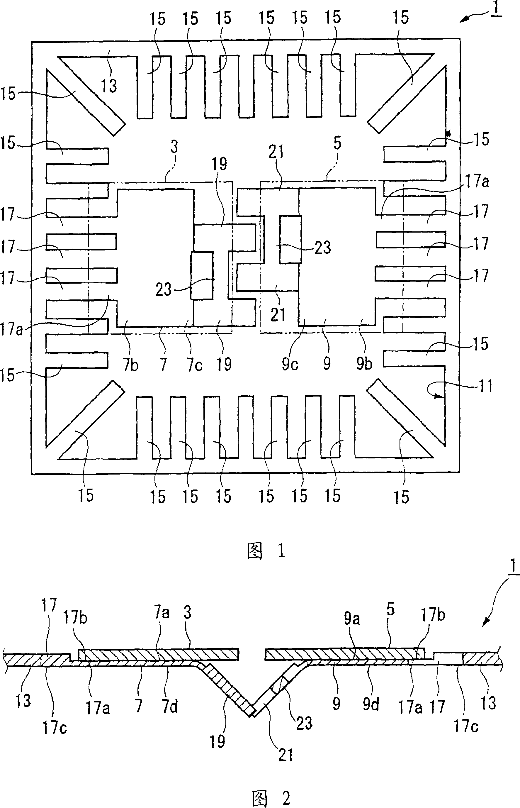
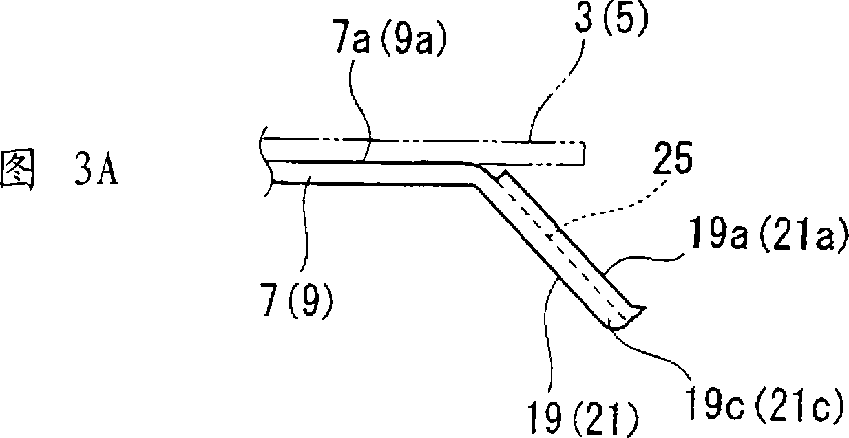
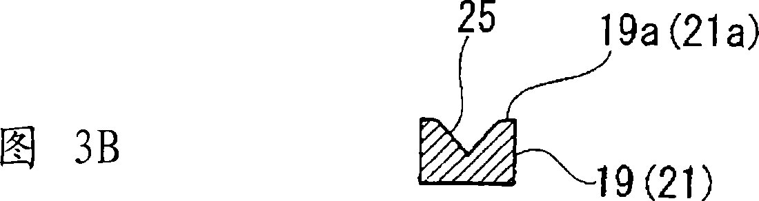
[0180] As shown in FIGS. 31 and 32, the lead frame 101 has two table portions 107, 109 for arranging magnetic sensor chips (physical quantity sensor chips) 103, 105 formed in a rectangular shape in plan view; frame portions supporting the table portions 107, 109 111; Connecting parts 119, 121 of the table parts 107, 109 and the frame part 111. These table parts 107 and 109, frame part 111, and connection parts 119 and 121 are integrally formed. The frame portion 111 has a rectangular frame portion 113 formed in a rectangular frame shape in plan view, which surrounds the table portions 107 and 109, and a plurality of lead wires 115 and 117 protruding inward from the rectangular frame portion 113. The connecting portions 119 and 121 connect the respective base portions 107 and 109 and the lead wires 117 (three wires each in this embodiment).
[0181] The lead wires 115 and 117 are electrically connected to the pads (not shown) of the magnetic sensor chips 103 and 105 and are arranged separately from each other. The two table portions 107 and 109 are arranged side by side along one side of the rectangular frame portion 113. The lead wire 117 connected to the table portions 107 and 109 extends in the arrangement direction of the two table portions 107 and 109. The lead wires 117 connected to the respective base portions 107 and 109 extend in directions opposite to each other.
[0182] Each of the base portions 107, 109 and the connecting portions 119, 121 is composed of a plurality of extension wires 123, 125 extending from the tip of each wire 117, and the respective extension wires 123, 125 are separated from each other. On the front ends of the extension wires 123 and 125 facing each other, there are formed protruding wires 127 and 129 that protrude toward the base portions 107 and 109 of each other. These protruding wires 127 and 129 are formed integrally with the wires 117 connecting the respective base portions 107 and 109. In addition, the protruding lead wires 127 and 129 do not overlap with the magnetic sensor chips 103 and 105 in a state where the magnetic sensor chips 103 and 105 are placed on the table portions 107 and 109.
[0183] Photolithography is performed on the surfaces 123a, 125a, 127a, and 129a of the extension wires 123, 125 and the protruding wires 127, 129. The protruding piece described is thin.
[0184] On the surfaces 123a, 125a of each extension lead 123, 125, a sheet-shaped insulating film 131, 133 is respectively arrange|positioned at the position corresponding to each of the mesa 107, 109. That is, the respective insulating films 131 and 133 are arranged on the plurality of extension wires 123 and 125. The insulating films 131 and 133 are formed of an electrically insulating material.
[0185] Adhesive layers (not shown) are formed on the front and back surfaces of the insulating films 131 and 133 in advance. The adhesive layer is formed on both sides of the insulating films 131 and 133 to bond the stage parts 107 and 109 and the magnetic sensor chips 103 and 105. The bonding layer has any function of temporary bonding that can be re-bonded after bonding or permanent bonding that cannot be re-bonded after bonding. The insulating films 131 and 133 are bonded to the table portions 107 and 109. In this state, the magnetic sensor chips 103 and 105 are bonded to the surfaces 123a and 125a of the table portions 107 and 109 via the insulating films 131 and 133.
[0186] On the front ends of the protruding wires 127 and 129 facing each other, protruding pieces 135 and 137 protruding toward the back surfaces 123d and 125d of the respective extension wires 123 and 125 are respectively formed.
[0187] In order to bend the protruding pieces 135 and 137 with respect to the extension wires 123 and 125 or the protruding wires 127 and 129, the base end portions of the protruding pieces 135 and 137 are photolithographically processed to obtain the same thickness as the mesa portions 107 and 109. In other words, the base end portions of the protruding pieces 135 and 137 are thinner than the other portions and can be deformed. Thereby, the inclination angle of the protruding pieces 135, 137 with respect to the table portions 107, 109 can be set with high accuracy.
[0188] Next, a method of manufacturing a magnetic sensor using the lead frame 101 described above will be described with reference to FIG. 35.
[0189] First, the magnetic sensor chips 103, 105 are bonded to the surfaces 123a, 125a of the mesa 107, 109 via the insulating films 131, 133. Next, the bonding wires 138 electrically connect the pads (not shown) arranged on the surfaces of the magnetic sensor chips 103 and 105 and the wires 115 and 117. In addition, the pad of one magnetic sensor chip 103 and the surface 129 a of the protruding wire 129 on the side of the mesa 9 where the other magnetic sensor chip 105 is arranged are similarly soldered with a wire 138.
[0190] In this case, the same wire 117 is electrically connected to the two magnetic sensor chips 103 and 105, and the wire 117 is used as a ground electrode or the like as an electrode shared by the two magnetic sensor chips 103 and 105, for example.
[0191] In addition, at the stage of tilting the stage portions 107 and 109, since the distance between the soldered portions of the magnetic sensor chips 103 and 105 and the soldered portions of the lead wires 115 and 117 varies, the material of the wire 138 is preferably a flexible and flexible material.
[0192] Next, the magnetic sensor chips 103 and 105 form a resin mold part that integrally fixes the base parts 107 and 109 and the lead wires 115 and 117.
[0193] That is, first, as shown in FIG. 33, the rectangular frame portion 113 of the lead frame 101 is arranged on the surface E102 of the mold E having the recessed portion E101. At this time, the lead wires 115, 117, the table portions 107, 109, the magnetic sensor chips 103, 105, and the protruding pieces 135, 137 inside the rectangular frame portion 113 are arranged above the recess E101. In addition, from the concave portion E101 side to the upper side, the magnetic sensor chips 103 and 105, the table portions 107 and 109, and the protruding pieces 135 and 137 are arranged in this order.
[0194] Above the protruding pieces 135 and 137, a metal mold F having a flat surface F101 is arranged, and the rectangular frame portion 113 of the lead frame 101 is clamped together with the metal mold E.
[0195] As shown in FIG. 34, when the rectangular frame portion 113 is clamped by the pair of upper and lower molds E, F, the flat surface F101 of the mold F presses the tip portions 135a, 137a of the protruding pieces 135, 137. At this time, the connecting parts 119 and 121 connected to the respective base parts 107 and 109 are deformed, and the base parts 107 and 109 are inclined with respect to the respective lead wires 117 around the reference axis L101 connecting the respective connecting parts 119 and 121 to each other. Here, the connecting portions 119 and 121 are formed thinner by photolithography and become easily deformable portions that are easily deformed. Therefore, the terrace portions 107 and 109 are inclined. Thus, together with the table portions 107 and 109, the magnetic sensor chips 103 and 105 are inclined at a predetermined angle with respect to the rectangular frame portion 113 or the flat surface F101.
[0196] After that, while pressing the tip portions 135a, 137a of the protruding pieces 135, 137 by the flat surface F101 of the mold F, molten resin is injected into the molds E, F, and the magnetic sensor chips 103, 105 are embedded in the resin. . Therefore, as shown in FIGS. 35 and 36, the magnetic sensor chips 103 and 105 are fixed to the inside of the resin mold part 141 in a mutually inclined state.
[0197] In addition, the resin used here is preferably a material with good fluidity so that the flow of the resin does not change the inclination angles of the magnetic sensor chips 103 and 105 and the stages 107 and 109.
[0198] Finally, the rectangular frame portion 113 is cut, and the wires 115 and 117 are respectively cut and electrically separated to complete the manufacture of the magnetic sensor 140.
[0199] In the magnetic sensor 140 manufactured as described above, as shown in FIG. 36, the arrangement relationship of the magnetic sensor chips 103 and 105 is the same as that described in the first embodiment. In addition, the magnetic sensor 140 has the same function as the first embodiment.
[0200] In addition, in the lead frame 101 and the magnetic sensor 140 described above, insulating films 131, 133 are provided between the magnetic sensor chips 103, 105 and the stage portions 107, 109, so the magnetic sensor chips 103, 105 and the stage portions 107, 109 are provided with insulating films 131, 133. The wire 117 connected by 109 is electrically insulated. Therefore, the electrical connection of the magnetic sensor chips 103 and 105 through the bonding wires can be performed not only by the wire 115 but also by the wire 117 constituting the stage portions 107 and 109. That is, the size of the lead frame 101 due to the increase in the number of wires 115 will not increase, and the number of wires that are possible for electrical connection with the magnetic sensor chips 103 and 105 can be increased.
[0201] That is, in the first embodiment, the lead wire 17 used for connection with the stage portions 7 and 9 is used for the electrical connection with the magnetic sensor chips 103 and 105 of this embodiment. Therefore, more input and output can be performed with respect to the magnetic sensor chips 3 and 5, and as a result, a high-performance magnetic sensor 40 can be provided.
[0202] In addition, it is not necessary to separately provide a lead wire dedicated to connection with the table portions 107 and 109 on the frame portion 111. Compared with the case where a wire dedicated for connection is provided, the size of the frame portion 111 surrounding the table portions 107 and 109 can be reduced, and the size of the magnetic sensor 40 can be reduced.
[0203] In addition, a wire 138 is soldered between the pad of one magnetic sensor chip 103 and the surface 129a of the protruding wire 129 on the side of the mesa 109 where the other magnetic sensor chip 105 is mounted. The same wire 117 can be connected to the two magnetic sensor chips 103, 105 Electric connection. As a result, the number of wires 117 used for electrical connection with the magnetic sensor chips 103 and 105 can be reduced, and the magnetic sensor 140 can be further miniaturized.
[0204] In addition, when the table portions 107, 109 and the magnetic sensor chips 103, 105 are inclined with respect to the frame portion 111 about the reference axis L101, the one end 103b of the one magnetic sensor chip 103 and the protruding wire 129 on the other magnetic sensor chip 105 side The distance is basically unchanged. Therefore, the wire 138 connected to the protruding wire 129 can be formed short, and the manufacturing cost of the magnetic sensor 140 can be reduced.
[0205] In addition, the base portions 107 and 109 and the connecting portions 119 and 121 are formed by the extension wires 123 and 125 of the same shape as the wire 117, so that the shape of the lead frame 101 can be simplified. Therefore, the manufacturing cost of the lead frame 101 or the magnetic sensor 140 can be reduced.
[0206] In addition, the magnetic sensor chips 103, 105 are bonded to the surfaces 123a, 125a of the table portions 107, 109 using the insulating films 131, 133 with adhesive layers. Therefore, compared with the conventional case of applying adhesives, The effect of easily improving the thickness accuracy of the adhesive layer can be achieved. Therefore, the inclination of the magnetic sensor chips 103, 105 with respect to the surfaces 123a, 125a of the table portions 107, 109 due to uneven thickness of the adhesive can be suppressed.
[0207] In addition, when a liquid adhesive is used for bonding the stage parts 107, 109 and the magnetic sensor chips 103, 105, there is a drop of liquid, and the liquid adhesive adheres to the surface of the lead 117 or the protruding lead 127, 129 The danger on 127a, 129a. In this embodiment, by using the insulating films 131, 133 with adhesive layers, no adhesive is attached to the surface of the wire 117 or the protruding wires 127, 129. Therefore, the magnetic sensor 40 can be easily manufactured.
[0208] In addition, in the above-mentioned embodiment, the wire 117 connected to the stage 109 and the magnetic sensor chip 103 mounted on the other stage 107 are electrically connected by the wire 38, but it is not limited to this. For example, as shown in FIGS. 37 and 38, the magnetic sensor chips 103 and 105 mounted on the respective base portions 107 and 109 and the protruding wires 126 and 128 extending from the same base portion may be electrically connected by wires 139 . These protruding wires 126 and 128 are formed at the tips of the respective extension wires 123 and 125 in an area that does not overlap the magnetic sensor chips 103 and 105.
[0209] In the case of this structure, after the protruding wires 126, 128 and the magnetic sensor chips 103, 135 are electrically connected by bonding wires, when the platform portions 107, 109 are tilted relative to the wire 117, the respective extension wires 123, 125 and the protruding wires 126, 128 The positional relationship does not change. Therefore, the deformation of the wire 139 connected between the magnetic sensor chips 103 and 105 and the protruding wires 126 and 128 can be reliably prevented. Therefore, the wire 139 can be formed short in advance, and the manufacturing cost of the magnetic sensor can be reduced.
[0210] In addition, the physical quantity sensor chips 103, 105 are electrically connected to the plurality of protruding wires 126, 128 constituting the table portions 107, 109, so the number of wires that can be electrically connected to the magnetic sensor chips 103, 105 can be further increased. That is, the plurality of lead wires 117 connected to the stage portions 107 and 109 can be used for electrical connection with the respective magnetic sensor chips 103 and 105, so that the magnetic sensor can be further miniaturized.
[0211] In addition, in the third embodiment described above, the extension cords 123 and 125 have the functions of all the platform portions 107 and 109, but extension cords that do not have the function as the platform portions 107 and 109 may be provided.
[0212] That is, for example, as shown in Figs. 37 and 38, the lead frame 146 has a first lead 143 (equivalent to the lead 117 shown in Fig. 31) that connects the extension leads 123 and 125 forming the mesa 107 and 109. In addition, the lead frame 146 has a second lead 144 arranged along the reference axis L101 together with the lead 143. On the wire 144, an adjacent wire 145 extending from the front end thereof is formed.
[0213] The adjacent wire 145 is arranged substantially parallel to the extension wires 123 and 125 at a certain interval, which is approximately equal to the length of the extension wire 123 plus the protruding wire 126. On the front end of the adjacent wire 145, a protruding piece 147 similar to the protruding pieces 135, 137 formed on the front end of the protruding wire 126, 128 is formed. The adjacent lead wires 145, like the extension lead wires 123 and 125, can be bent and inclined with respect to each of the second lead wires 144 with the reference axis L101 as the center. That is, the adjacent wire 145 may be inclined in the same direction and inclination angle as the extension wires 123 and 125.
[0214] When manufacturing a magnetic sensor using the lead frame 146, first, the magnetic sensor chips 103 and 105 are electrically connected to the adjacent wires 145 by bonding wires. After that, the protruding piece 147 is pressed by a metal mold, and the extension leads 123 and 125 and the adjacent lead 145 are inclined in the same direction. At this time, the relative distance between the adjacent wire 145 and the extension wires 23 and 25 is kept constant. That is, the wire 148 electrically connecting the magnetic sensor chips 103 and 105 and the adjacent wire 145 is not deformed, and the wire 148 can be formed in a short length. Therefore, the manufacturing cost of the magnetic sensor can be reduced.
[0215] In addition, since the adjacent lead wires 145 and the stages 107 and 109 can be inclined at the same inclination angle, chips larger than the magnetic sensor chips 103 and 105 can be mounted on the stages 107 and 109. That is, a larger chip can also be supported by the adjacent wire 145. As shown, there is no need to change the design of the lead frame 146 corresponding to the size of the magnetic sensor chip, and the lead frame 146 can be used universally. In this case, it is preferable to provide insulating films 131 and 133 between the magnetic sensor chip and the adjacent wire 145 as well.
[0216] In addition, since the adjacent wires 145 have the same shape as the extension wires 123 and 125, the lead frame 46 is easy to manufacture.
[0217] In addition, in the lead frame 146 of the above embodiment, the two stage portions 107 and 109 are designed to incline with the reference axis L101 parallel to each other as the center, but it is not limited to this. For example, as shown in FIG. 39, it is also possible to design so that the two table parts 107, 109 may incline centering on the reference axis|shaft L101, L102 which are mutually perpendicular. In this structure, the wires 117 forming the respective mesa portions 107 and 109 are perpendicular to each other. In this case, the two sensing directions (the A direction and the C direction) perpendicular to each other of the two magnetic sensor chips 103 and 105 are arranged in a plane parallel to the lower surface 141a of the resin mold portion 141, so that the measurement can be performed with high accuracy. Magnetic along 141a below.
[0218] In addition, in the structure shown in FIG. 39, two magnetic sensor chips 103 and 105 are arranged along a diagonal line L103 of the rectangular frame portion 113. According to this configuration, the flow of the molten resin can be smoothly performed when the table portions 107, 109, the magnetic sensor chips 103, 105, and the lead wires 115, 117 are integrally molded by the resin.
[0219] That is, when the molten resin is poured into the resin forming space formed by the metal molds E and F to form the resin molded part 141, it passes through the rectangular frame part 113 located on the diagonal line L104 intersecting the diagonal line L103. One corner portion 113a flows into the other corner portion 113b with molten resin, and the table portions 107, 109 or the magnetic sensor chips 103, 105 will not hinder the flow of the molten resin.
[0220] Therefore, the molten resin can smoothly reach the other corner 113b from one corner 113a, and poor resin filling can be reliably prevented. In addition, it is possible to prevent the table parts 107 and 109 or the magnetic sensor chips 103 and 105 from being subjected to flow pressure due to the flow of the molten resin, and their inclination angles can be prevented from changing. As a result, the inclination angle of the magnetic sensor chips 103 and 105 can be accurately set.
[0221] In addition, in this embodiment, the same lead wire as the adjacent lead wire 145 described in FIG. 37 may be provided at the tip of the lead wire 115 arranged together with the lead wire 117 forming the mesa portions 107 and 109.
[0222] In addition, an example of using insulating films 131 and 133 with adhesive layers formed on the front and back surfaces is illustrated, but the thickness of the adhesive layer is not limited to this, and the insulating films may also be bonded with an adhesive. And the stages 107 and 109 and the magnetic sensor chips 103 and 105.
[0223] In addition, the protruding pieces 135, 137, and 147 are not limited to being formed on the opposing platform portions 107, 109 or the end adjacent to the lead 145, as long as they protrude toward at least the back surfaces 123d, 125d of the platform portions 107, 109.
[0224] In addition, the table portions 107, 109 or the adjacent wires 145 are inclined by the protruding pieces 135, 137, and 147, but it is not limited to this. At least at the end of the manufacturing stage of the magnetic sensor 140, the two magnetic sensor chips 103, 105 or the adjacent wires 145 may be tilted by other methods.

Example

[0225] (Fourth embodiment)
[0226] Figures 40 to 45 show the fourth embodiment of the present invention. The magnetic sensor (physical quantity sensor) of this embodiment is the same as the above-mentioned embodiment. The direction and magnitude of the external magnetic field are measured by two magnetic sensor chips inclined to each other. It is manufactured by a lead frame formed by press processing or etching processing.
[0227] The lead frame 201, as shown in FIGS. 40 and 41, has two table portions 207, 209 on which magnetic sensor chips (physical quantity sensor chips) 203, 205 formed in a rectangular shape in plan view are mounted; frames supporting the table portions 207, 209部211. These table parts 207 and 209 and the frame part 211 are integrally formed. The frame portion 211 is composed of the following components, surrounds the table portions 207 and 209, and is formed as a rectangular frame portion 213 having a substantially square frame portion in plan view; from each side 213a to 213h of the inner region S201 of the rectangular frame portion 213, it faces vertically A plurality of lead wires 215 and 216 protruding inside; a connecting lead wire (connecting portion) 217 ​​protruding inward from the corners 213e to 213h of the inner region S201.
[0228] A plurality of lead wires 215 and 216 are respectively provided on each side 213a to 213d of the inner region S201 (each 7 wires in the example of the figure). The wires 215 and 216 are provided for electrically connecting the pads (not shown) of the magnetic sensor chips 203 and 205. In addition, the lead wires 215 and 216 are arranged only in the middle of the sides 213a to 213d of the inner region S201 in order to avoid contact with the connecting wires 217 described later, and are not provided at the ends of the sides 213a to 213d. The corners 213e to 213h of the inner region S201 become non-installed regions S202 to S205 where the wires 215 and 216 are not provided.
[0229]The connecting wire 217 is a hanging wire connecting the platform portions 207 and 209 and the rectangular frame portion 213. One end portion 217a of the connecting lead wire 217 is connected to the side end portions located at both ends of the one end portions 207a and 209a of each of the base portions 207 and 209. Here, the side end portions of the respective table portions 207 and 209 refer to the end portions of the respective table portions 207 and 209 perpendicular to the parallel direction of the two table portions 207 and 209. One end 217a of the connecting wire 217 is provided with a concave cutout on its side surface, which is formed thinner than the other parts. This cutout becomes a twisted portion that can be easily deformed when the respective base portions 207 and 209 are bent and inclined around the axis L201 of the two parallel sides 213a and 213c of the inner region S201 as the center.
[0230] The two stage parts 207 and 209 are arranged side by side along one side 213d of the inner region S201. In addition, the respective base portions 207 and 209 are shifted relative to the lead wires 215 and 216 in the thickness direction of the metal thin plate (lead frame). The surfaces 207b and 209b of the table portions 207 and 209 are respectively formed in a substantially rectangular shape in a plan view to mount the magnetic sensor chips 203 and 205. These two stages 207 and 209 are respectively arranged at positions closer to the non-installation areas S202 and S205 than the non-installation areas S203 and S204, and their surfaces 207b and 209b are smaller than the mounting surfaces of the magnetic sensor chips 203 and 205.
[0231] From the tip portion 215a of the wire 215 adjacent to the end portions 207a, 209a of the mesa portions 207, 209 to the surface 215b of the intermediate portion, a recess 220 is formed by photolithography, that is, the thickness of the tip portion 215a of the wire 215, It is formed thinner than the base end part 215c of the lead wire 215 located on the side of the rectangular frame part 213.
[0232] On the other end portions 207c, 209c of the table portions 207, 209, a pair of protruding pieces 219, 221 protruding toward the back surfaces 207d, 209d of the table portions 207, 209 are respectively formed. These protruding pieces 219 and 221 are provided for tilting the table portions 207 and 209. The protruding piece 219 of the table portion 207 and the protruding piece 221 of the table portion 209 are opposed to each other. In order to stably incline each of the table parts 207 and 209, it is preferable to make the distance between the pair of protruding pieces 219 and 221 formed on each of the table parts 207 and 209 large.
[0233] In addition, in order to stabilize the inclination angle of each of the table portions 207 and 209, it is desirable to enlarge the width of the front end portions of the pair of projecting pieces 219 and 221. As a result, since the area of ​​the tip portion that receives the pressing force when each of the table portions 207 and 209 is inclined increases, the deformation of the protruding pieces 219 and 221 is prevented by stress relaxation, and the inclination of the table portions 207 and 209 is stabilized. Specifically, the pair of protruding pieces 219 and 221 may have a wider width instead of the rod shape shown in the figure. Alternatively, the tip of each protruding piece 219, 221 may be bent into a rectangular shape.
[0234] The two table portions 207 and 209 are arranged close to the same side 203d side of the inner region S201, and therefore, the inner region S201 located on the side 203b side opposite to the side 203d becomes the remaining region. On this remaining area, a substantially rectangular auxiliary table portion 223 connected to the connecting wire 217 is formed.
[0235] As shown in FIG. 42, the auxiliary table portion 223 is shifted in the thickness direction of the metal thin plate (lead frame 201) in the same way as the table portions 207 and 209. The auxiliary table portion 223 is formed with a torsion portion 217b and a pair of protruding portions 225 for tilting about an axis L202 perpendicular to the aforementioned axis L201 as a center. On the surface 223a of the auxiliary table portion 223, a semiconductor chip 227 such as a magnetic sensor chip, an acceleration sensor chip, a temperature sensor chip, a signal processing LSI, and the like as described above is mounted. The semiconductor chip 227 is electrically connected to a wire 216 arranged around it.
[0236] Next, a method of manufacturing a magnetic sensor using the lead frame 201 described above will be described.
[0237] As shown in FIGS. 40 to 42, first, the magnetic sensor chips 203, 205 and the semiconductor chip 227 are bonded to the surfaces 207b, 209b, and 223a of the table portions 207, 209 and the auxiliary table portion 223. The magnetic sensor chips 203 and 205 are arranged close to the non-installation regions S202 and S205 and their sides are parallel to the sides 213a to 213d of the inner region S201. In addition, each magnetic sensor chip 203, 205 is exposed from the surfaces 207b, 209b of the table portions 207, 209, and this exposed portion is not provided with the plurality of lead wires 215, 216 provided on the sides 213a, 213c of the inner region S201. The plurality of conductive wires 215 (four in the example of the figure) on the side of the regions S202 and S205 are arranged so as to overlap. As shown in FIG. 41, the stage portions 207 and 209 are offset from the lead 215 in the thickness direction of the metal thin plate (lead frame 201). Therefore, the magnetic sensor chips 203 and 205 are not in contact with the lead 215.
[0238] The magnetic sensor chips 203 and 205 are arranged in a region from the tip part 215a of the wire 215 formed thinly by the above-mentioned photolithography process to the middle part. In addition, the magnetic sensor chips 203 and 205 are arranged so as not to overlap the lead wires 216 arranged in the arrangement direction (side 213d) of the table portions 207 and 209.
[0239] Then, the pads (not shown) arranged on the surfaces of the magnetic sensor chips 203 and 205 and the semiconductor chip 227 and the wires 216 that do not overlap with the magnetic sensor chips 203 and 205 are electrically connected by wires (not shown). In addition, the positional relationship between the soldered portions of the magnetic sensor chips 203, 205 and the semiconductor chip 227 and the soldered portion of the lead wire 216 changes at the stage where the stage portions 207, 209 and the auxiliary stage portion 223 described later are tilted. Therefore, the material of the wire A flexible and soft material is preferred.
[0240] Next, a resin mold part (package) for integrally fixing the magnetic sensor chips 203 and 205, the semiconductor chip 227, the stage parts 207 and 209, the auxiliary stage part 223, and the wires 215 and 216 is formed.
[0241] That is, as shown in FIG. 43, the rectangular frame portion 213 of the lead frame 201 is positioned on the surface E202 of the mold E having the recessed portion E201. At this time, the lead wires 215, 216, the table portions 207, 209, the magnetic sensor chips 203, 205, and the protruding pieces 219, 216 inside the rectangular frame portion 213 are arranged above the recess E201. That is, in this state, the magnetic sensor chips 203 and 205, the table portions 207 and 209, and the protruding pieces 219 and 221 are arranged in this order from the concave portion E201 side to the upper side.
[0242] Above the protruding pieces 219 and 221, a metal mold F having a flat surface F201 is arranged, and the rectangular frame portion 213 of the lead frame 201 is clamped together with the metal mold E.
[0243] As shown in FIG. 44, when the rectangular frame portion 213 is clamped by the pair of metal molds E and F, the projecting pieces 219, 221 are pressed by the flat surface F201 of the metal mold F. With this pressing force, one end 217a of the connecting lead 217 is twisted with the axis L201 as the center, and the table portions 207 and 209 are inclined. At this time, the one ends 203 a and 205 a of the magnetic sensor chips 203 and 205 facing the surface 215 b of the lead wire 215 enter the recess 220. Thus, together with the table portions 207 and 209, the magnetic sensor chips 203 and 205 are inclined at a predetermined angle with respect to the rectangular frame portion 213 or the flat surface F201.
[0244] The auxiliary table portion 223, like the table portions 207 and 209, is inclined by a predetermined angle with respect to the rectangular frame portion 213 or the flat surface F201 by pressing the protruding piece 225 by the flat surface F201 of the mold F.
[0245] After that, while the protruding pieces 219 and 221 are pressed by the flat surface F201 of the metal mold F, molten resin is injected into the resin forming space formed by the recesses E201 and the flat surface F201 of the metal molds E and F. This molten resin forms a resin mold part in which the magnetic sensor chips 203 and 205 are embedded in the resin. After the resin is cured, as shown in FIGS. 45 to 47, the magnetic sensor chips 203 and 205 are fixed to the inside of the resin mold (package) 229 in a state of being inclined to each other. The resin used here is preferably a material with good fluidity so that the flow of the resin does not cause the inclination angle of the magnetic sensor chips 203 and 205 and the semiconductor chip 227 to change.
[0246] Finally, the rectangular frame portion 213 is cut off, and the wires 215 and 216 and the connecting wire 217 are respectively cut to complete the manufacture of the magnetic sensor 230.
[0247] The resin mold portion 229 of the magnetic sensor 230 manufactured as described above is formed in a rectangular shape in plan view similar to the rectangular frame portion 213 described above. The lead wires 215 and 216 extend from the sides 229 d to 229 g of the inner region S201 divided by the resin mold portion 229 toward the inner side of the resin mold portion 229. These lead wires 215 and 216 are not provided in the non-installation regions S202 to S205 located at the corners of the inner region S201.
[0248] The back surface 216a of the lead wire 216 is exposed from the lower surface 229a side of the resin mold portion 229. One ends of these lead wires 216 are electrically connected to the magnetic sensor chips 203 and 205 and the semiconductor chip 227 through metal wires (not shown), and these connection portions and wires are embedded in the resin mold portion 229.
[0249] Referring to FIG. 46, the magnetic sensor chips 203 and 205 and the semiconductor chip 227 are inclined with respect to the lower surface 229a of the resin mold portion 229. The other end portions 203 b and 205 b of the magnetic sensor chips 203 and 205 facing each other face the upper surface 229 c side of the resin mold portion 229. The surface 203a of the magnetic sensor chip 203 is inclined at an acute angle with the surface 205a of the magnetic sensor chip 205 as a reference. That is, the angle θ of the table portion 207 with respect to the table portion 209 is an acute angle.
[0250] Therefore, the sensing directions of the magnetic sensor chips 203 and 205 are the same as those of the first embodiment of the present invention described using FIG. 7. In addition, the angle θ formed by the AB plane with respect to the CD plane is theoretically larger than 0° and less than 90° to measure the three-dimensional geomagnetic orientation, but in practice, it is preferably greater than 20°, and more preferably 30° or more. This point is the same as the first embodiment.
[0251] This magnetic sensor 330, like the magnetic sensor 30 of the first embodiment, is mounted on a substrate in a portable terminal device, for example, and can detect the orientation of the geomagnetism.
[0252] With the lead frame 201 and the magnetic sensor 230 described above, since a part of the magnetic sensor chips 203 and 205 and the lead 215 are arranged to overlap, the size of the magnetic sensor 230 can be reduced.
[0253] In addition, the magnetic sensor chips 203 and 205 are arranged close to one corner of each inner region, that is, the regions S202 and S205 are not provided, and are arranged so as to overlap only the lead wires 15 protruding from the sides 213a and 213c of the inner region S201. Therefore, compared with the case where the stage portions 207 and 209 or the magnetic sensor chips 203 and 205 are arranged at the central portion of the sides 213a and 213c of the inner region S201, the number of wires overlapping with the magnetic sensor chips 203 and 205 is reduced. Therefore, without changing the arrangement of the wires 215 and 216 with respect to the rectangular frame portion 213, the number of wires 216 that can be electrically connected to the magnetic sensor chips 203 and 205 can be sufficiently ensured. Therefore, more signal input and output can be performed with respect to the magnetic sensor chips 203 and 205, and a high-performance magnetic sensor 230 can be provided.
[0254] In addition, since there is no need to change the arrangement of the wires 215 and 216 with respect to the rectangular frame portion 213, the high-performance magnetic sensor 230 can be manufactured easily and inexpensively.
[0255]In addition, by arranging the two table portions 207, 209 or the magnetic sensor chips 203, 205 close to the same side 213d, 229g of the inner region S201, it is possible to additionally arrange a new one on the remaining area of ​​the inner region S201 of the rectangular frame portion 213 The auxiliary stage 223 or the semiconductor chip 227 can provide a higher performance magnetic sensor 230 without changing the size of the rectangular frame 213 or the resin mold 229.
[0256] In addition, the inclined magnetic sensor chips 203, 205 can enter the recess 220 formed on the surface 215b of the wire 215, and therefore, it is not necessary to extend in the thickness direction of the metal thin plate to shift the length of the base portions 207, 209 relative to the wire 215. The magnetic sensor chips 203 and 205 and the lead wire 215 are prevented from contacting, and the magnetic sensor chips 203 and 205 are largely tilted with respect to the frame portion 211. Therefore, the thickness of the magnetic sensor 230 can be reduced.
[0257] In addition, in the above-described embodiment, the protruding piece 225 is provided on the auxiliary table portion 223, but it is not limited to this. The auxiliary table portion 223 may be inclined with respect to the frame portion 11 at least before the resin mold portion 29 is formed.
[0258] In addition, the auxiliary table 223 does not need to be tilted when the semiconductor chip 227 to be placed is a temperature sensor chip or a signal processing LSI. In this case, the protruding piece 225 and the twisted portion of the connecting lead 217 are not required.
[0259] Next, a fifth embodiment of the present invention will be described with reference to FIG. 48. Compared with the fourth embodiment, the lead frame and the magnetic sensor of the fifth embodiment differ in the positions of the table portion and the magnetic sensor chip relative to the frame portion. Here, only the arrangement of the stage part and the magnetic sensor chip will be described. The same reference numerals are used for the same parts as the components of the lead frame 201 or the magnetic sensor 230, and the description thereof will be omitted.
[0260] In the lead frame 231 and the magnetic sensor of this embodiment, the two stages 207 and 209 and the magnetic sensor chips 203 and 205 are arranged side by side on the diagonal line L203 of the inner region S201. The respective stage parts 207 and 209 are arranged close to the corners located on the diagonal line L203, that is, close to the non-installation areas S202 and S204.
[0261] When the magnetic sensor is manufactured using the lead frame 231, the rectangular frame portion 213 is clamped by the same metal mold as in the fourth embodiment, and the resin defined by the recesses E201 and the flat surface F201 of the metal molds E and F A molten resin is injected into the forming space to form a resin mold portion 229 in which the magnetic sensor chips 203 and 205 are embedded in the resin. The molten resin is ejected from the opening M on the side of one corner 213h of the rectangular frame portion 213 on the other diagonal line L204 intersecting the other diagonal line L203 in the inner region S201 of the rectangular shape, and is directed toward One corner 213h is opposite to the other corner 213f side of the flow.
[0262] In addition, the above-mentioned resin forming space corresponds to the inner region S201 defined by the resin mold part 229.

PUM

no PUM

Description & Claims & Application Information

We can also present the details of the Description, Claims and Application information to help users get a comprehensive understanding of the technical details of the patent, such as background art, summary of invention, brief description of drawings, description of embodiments, and other original content. On the other hand, users can also determine the specific scope of protection of the technology through the list of claims; as well as understand the changes in the life cycle of the technology with the presentation of the patent timeline. Login to view more.
Why Eureka
Try Eureka