

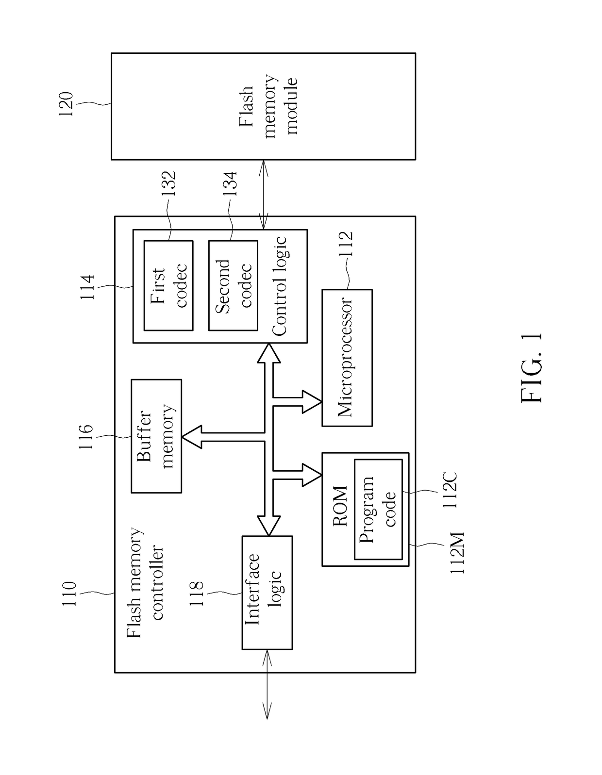
Flash memory controller and memory device for accessing flash memory module, and associated method
a flash memory module and controller technology, applied in the field of flash memory, can solve the problems of introducing some problems when writing/reading data, errors may occur on data of errors will occur on floating gate transistors of other word lines in the word line group, so as to save memory space
- Summary
- Abstract
- Description
- Claims
- Application Information
AI Technical Summary
Benefits of technology
Problems solved by technology
Method used
Image

Examples
first embodiment
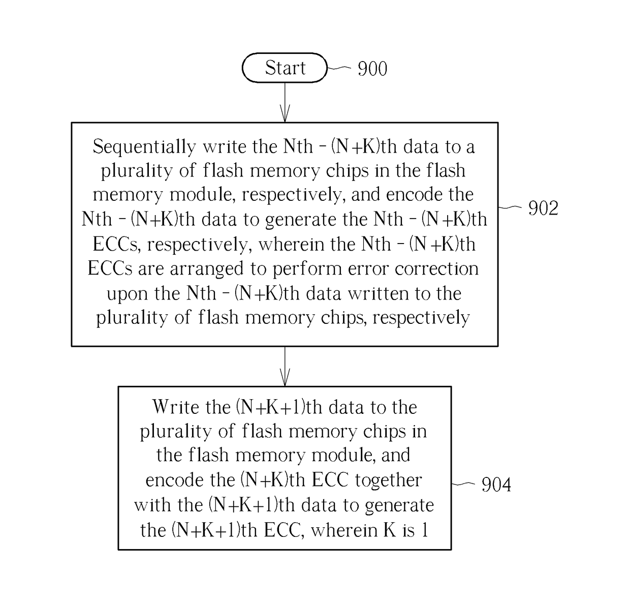
[0037]Refer to FIGS. 5 and 6, wherein FIG. 6 is a diagram illustrating the flash memory controller 110 writing data to the super block 530 according to the present invention. In the following descriptions, each data is written to a page of the flash memory chips 512, 514, 522 and 524. The first data will be written to the first page P0 of each of the flash memory chips 512, 514, 522 and 524, the second data will be written to the second page p1 of each of the flash memory chips 512, 514, 522 and 524, and the Nth data will be written to the Nth page P(N−1) of each of the flash memory chips 512, 514, 522 and 524. Referring to FIG. 6, when the flash memory controller 110 is going to write the first data to the super block 530, the second codec 134 in the flash memory controller 110 will encode the first data first to generate a first ECC S0, wherein the second codec 134 may adopt the Reed-Solomon (RS) encoding algorithm or an exclusive-OR (XOR) calculation to encode the data written to...
second embodiment
[0057]For better understanding, refer to FIGS. 4 and 5, which illustrate the flash memory controller 110 writing data to the super block 530. Refer to FIG. 8, which is a diagram illustrating the flash memory controller 110 writing data to the super block 530 according to the present invention. Note that, in the following descriptions of this embodiment, “data” refers to the data written to a word line group, rather than the data on a word line as shown in the embodiment of FIG. 6. When the flash memory controller 110 writes the first data to the super block 530 (as mentioned in the embodiment of FIG. 6), the second codec 134 in the flash memory controller 110 will encode the first data to generate the first ECCs S0-S3, write the first data to the pages P0-P3 in each of the flash memory chips 512, 514, 522 and 524, respectively, and store the ECCs S0-S3 into a specific block of the flash memory chips 512, 514, 522 or 524, wherein the specific block does not belong to the super block ...
third embodiment
[0071]For better understanding, refer to the examples shown in FIGS. 4-5, which show the flash memory controller 110 writing data to the super block 530. Refer to FIG. 10, which is a diagram illustrating the flash memory controller 110 writing data to a super block 530 according to the present invention. For brevity, in the following descriptions of this embodiment, the term “data” represents the data written to a word line group rather than the data originally existing in the word line as shown in FIG. 6. When the flash memory controller 110 needs to write the first data to the super block 530, as in the embodiment of FIG. 6, the second codec 134 in the flash memory controller 110 will encode the first data to generate the first ECCs S0-S3, write the first data to the pages P0-P3 of each of the flash memory chips 512, 514, 522 and 524, respectively, and store the ECCs S0-S3 into a specific block of the flash memory chips 512, 514, 522 or 524, wherein the specific block does not bel...
PUM
 Abstract
Description
Claims
Application Information