Check patentability & draft patents in minutes with Patsnap Eureka AI!

Methods of forming patterns of semiconductor devices

a technology of semiconductor devices and patterns, applied in the direction of photosensitive material processing, photomechanical equipment, instruments, etc., can solve the problems of complex methods, high cost, and difficulty in obtaining patterns with specific critical limits

Active Publication Date: 2018-10-16
SAMSUNG ELECTRONICS CO LTD +1
View PDF25 Cites 1 Cited by
  • Summary
  • Abstract
  • Description
  • Claims
  • Application Information

AI Technical Summary

Problems solved by technology

However, a pattern having a specific critical limit may be difficult to obtain due to a resolution limit.
Thus, a double patterning method (e.g., using at least two different masks) has been considered but such a method may be complicated and costly.

Method used


Image

  • Methods of forming patterns of semiconductor devices
  • Methods of forming patterns of semiconductor devices
  • Methods of forming patterns of semiconductor devices

Examples


experimental example 1

es of Brush Layers

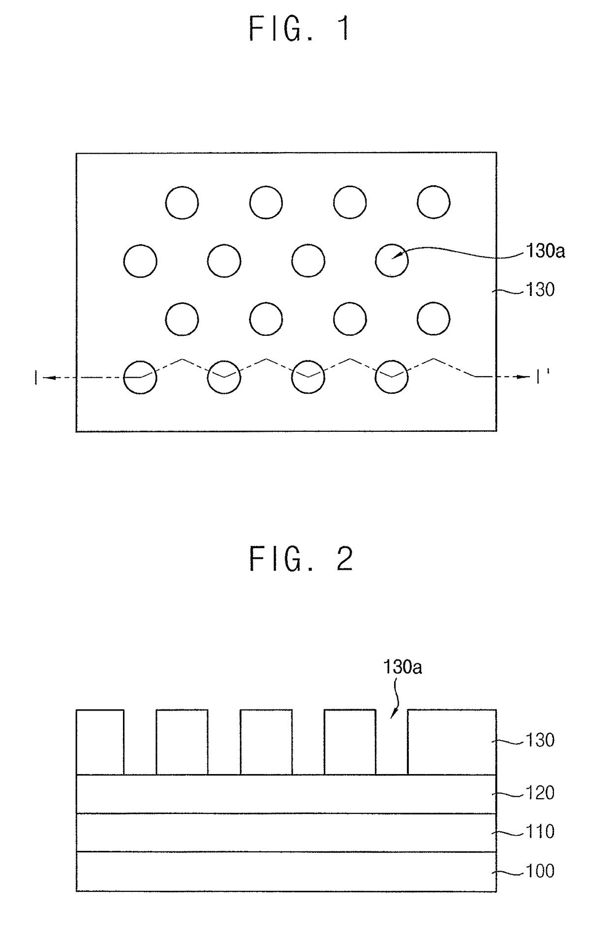
[0138]Guide patterns having a pillar shape were formed of silicon oxide on a silicon wafer. Brush layers using the brush polymers of Example 1 (PS-diOH brush polymer represented by the above Chemical Formula 3), Example 2 (PS-r-HEMA brush Polymer represented by the above Chemical Formula 5) and Comparative Example 1 (PS—OH brush polymer represented by Chemical Formula 6 below) were formed on surfaces of the guide patterns. A reaction temperature at which a thickness of each brush layer was saturated on the guide patterns was measured, and a contact angle with respect to water of the each brush layer having a saturated thickness was measured. The results are shown in Table 1 below.

[0139]

[0140]

TABLE 1Reaction TemperatureContact AngleComparativeabout 210° C. 85°Example 1Example 1about 180° C. to about 200° C.87.4°Example 2about 150° C. to about 180° C.86.1°

[0141]Referring to Table 1, each contact angle of Examples 1 and 2 was greater than that of Comparative Example 1...

experimental example 2

ignment Failures According to Types of Block Copolymers

[0143]Oxide guide patterns, each of which had a diameter of 70 nm, were formed. A self-aligned layer was formed using a lamellar-type block copolymer in which a volume ratio of PS and PMMA was 55:45. A unit length at which PMMA blocks of a pillar shape was observed was measured varying a unit length of the lamellar-type block copolymer. The PMMA blocks of the pillar shape were observed when the unit length reached about 50 nm. Thus, a self-alignment of the pillar shape was induced by controlling a ratio of the diameter of the guide patterns and the unit length of the block copolymer, even though the lamellar-type block copolymer was used.

[0144]Based on the results above, a brush layer of the PS-diOH structure having a thickness of 10 nm was formed on the oxide guide patterns. An alignment failure was evaluated using a pure lamellar-type PS-b-PMMA, and a blend of the lamellar-type block copolymer and homopolymers thereof. PMMA an...

experimental example 3

ignment Failures According to Types of Brush Layers and Block Copolymers

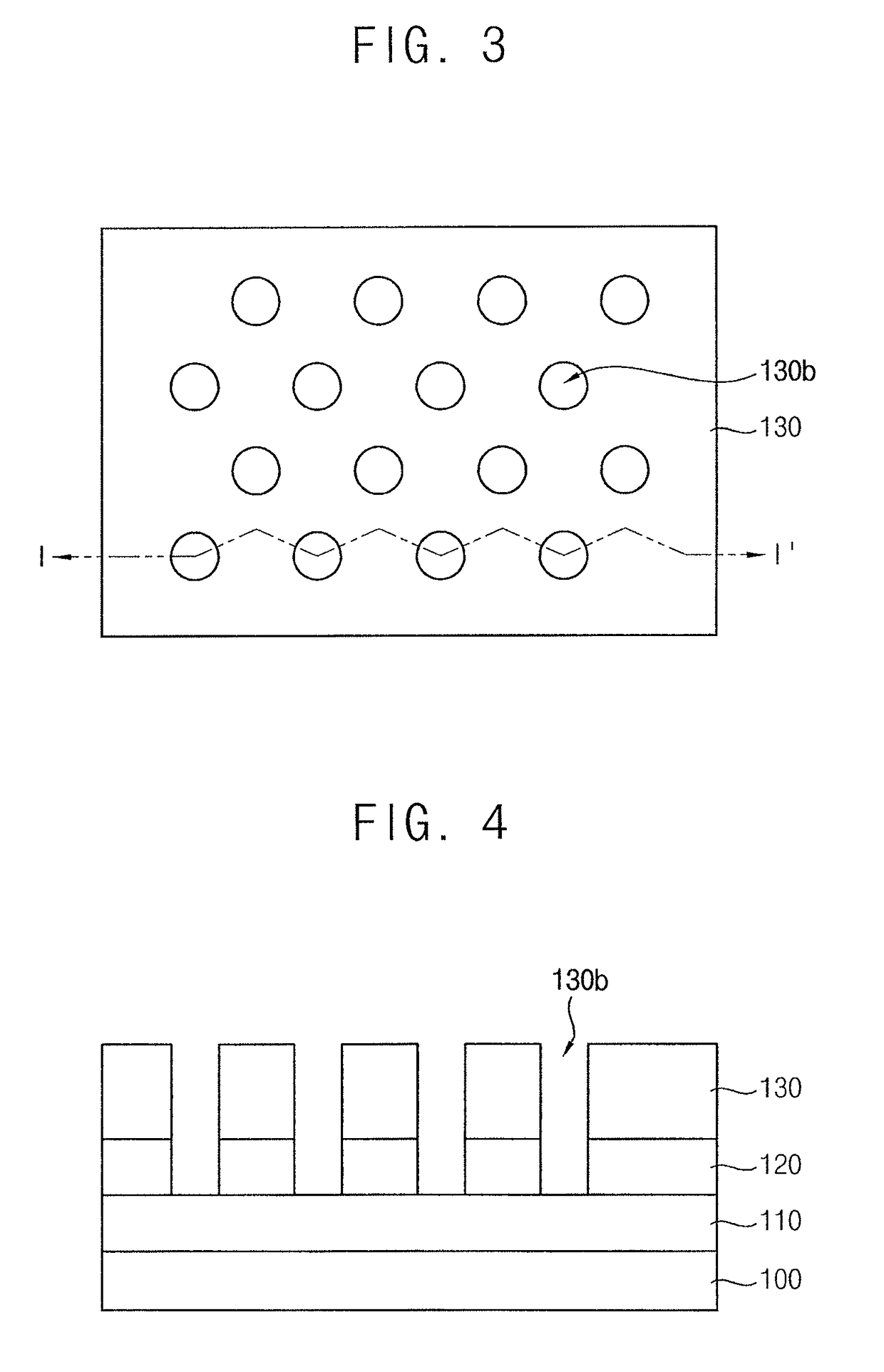
[0148]A silicon carbonitride (SiCN) layer was formed on a wafer, and oxide guide patterns each of which had a diameter of 70 nm were formed on the silicon carbonitride layer. A brush layer was formed on surface of the guide patterns, and a blend of a cylinder-type PS-b-PMMA (a volume ratio of PS and PMMA=7:3) and a blend of a lamellar-type PS-b-PMMA (a volume ratio of PS and PMMA=55:45) were phase-separated on the brush layer. PMMA pillars were removed to form holes, and the silicon carbonitride layer was etched through the holes, and then the number of not-open failures or bridges in a unit area of the wafer was measured. The results are shown in Table 2 below.

[0149]

TABLE 2Number ofBlock CopolymerBrush PolymerFailuresCylinder-TypePS-OH>125,000Ternary BlendPS-HEMA827PS-diOH4,802PS-HEMA (30 wt %) +655PS-diOH (70 wt %)PS-HEMA (70 wt %) +561PS-diOH (30 wt %)Lamellar-TypePS-HEMA929Ternary BlendPS-diOH361

[0150]Referr...


PUM

PropertyMeasurementUnit
temperatureaaaaaaaaaa
reaction temperatureaaaaaaaaaa

Abstract

In a method of forming patterns, an object layer is formed on a substrate. Guide patterns are formed on the object layer. A brush layer is formed using a brush polymer on surfaces of the guide patterns. The brush polymer includes at least one of a first brush polymer and a second brush polymer. The first brush polymer includes a hydrophobic repeating unit and a hydrophilic terminal group having at least two hydroxyl groups. The second brush polymer includes a hydrophobic repeating unit and a hydrophilic random repeating unit having a hydroxyl group. A self-aligned layer is formed using a block copolymer on the brush layer to form blocks aligned around the guide patterns. At least a portion of the blocks is transferred to the object layer.

Description

CROSS-REFERENCE TO RELATED APPLICATION[0001]Korean Patent Application No. 10-2015-0158213, filed on Nov. 11, 2015, in the Korean Intellectual Property Office, and entitled: “Methods of Forming Patterns of Semiconductor Devices and Methods of Manufacturing Semiconductor Devices,” is incorporated by reference herein in its entirety.BACKGROUND[0002]1. Field[0003]Embodiments relate to methods of forming patterns of semiconductor devices and methods of manufacturing semiconductor devices.[0004]2. Description of the Related Art[0005]In general photolithography, an exposure device has been developed for forming fine and minute patterns. However, a pattern having a specific critical limit may be difficult to obtain due to a resolution limit. Thus, a double patterning method (e.g., using at least two different masks) has been considered but such a method may be complicated and costly.SUMMARY[0006]Embodiments are directed to a method of forming patterns that includes forming an object layer o...

Claims


Application Information

Patent Timeline
Patent Type & Authority Patents(United States)
IPC IPC(8): G03F7/004G03F7/16H01L27/108C08F20/28B82Y10/00B82Y40/00C08L53/00G03F7/20G03F7/00G03F7/40H01L21/033H01L21/311H01L21/3213H01L49/02
CPCG03F7/165B82Y40/00C08F20/28C08L53/00G03F7/0002G03F7/0035G03F7/2022G03F7/2059G03F7/40H01L21/0337H01L21/31144H01L21/32139H01L27/10844H01L28/00B82Y10/00B81C2201/0149H10B12/01
Inventor PARK, JEONG-JUKWON, SEUNG-CHULKIM, EUN-SUNGLEE, KYEONG-MIYI, SHI-YONGKUROSAWA, TSUYOSHOHMORI, KATSUMIMATSUMIYA, TASUKU
Owner SAMSUNG ELECTRONICS CO LTD
Features
  • R&D
  • Intellectual Property
  • Life Sciences
  • Materials
  • Tech Scout
  • Unparalleled Data Quality
  • Higher Quality Content
  • 60% Fewer Hallucinations
Learn More