Array substrate and display device

a display device and substrate technology, applied in semiconductor devices, semiconductor/solid-state device testing/measurement, instruments, etc., can solve the problems of inability to directly implement contact measurement on tft performance after liquid crystal cell formation as well as electrical properties, pixels may be damaged, and it is impossible to acquire performance parameters of the tested tft after liquid crystal cell formation

Inactive Publication Date: 2019-01-01
BOE TECH GRP CO LTD +1
View PDF28 Cites 0 Cited by
  • Summary
  • Abstract
  • Description
  • Claims
  • Application Information

AI Technical Summary

Benefits of technology

[0029]In embodiments of the present invention, a test unit is arranged in a peripheral circuit region on the array substrate, so as to effectively avoiding the failing of testing internal TFT performance as well as properties such as capacitance after the display panel is cell-assembled in the prior art.

Problems solved by technology

Because both pixel and circuits on the array substrate are encapsulated internally after the array substrate is completed, it is impossible to directly implement contact measurement on TFT performance after the liquid crystal cell is formed as well as electrical properties such as capacitance in the liquid crystal cell.
However, the films may be scratched by a test probe, that is, pixels may be damaged by the method, and accordingly, this method is only suitable for testing pixel electrical properties before coating alignment layer (Polyimide film, i.e., PI film).
By using the test method mentioned above, it is impossible to acquire performance parameters of the tested TFT after liquid crystal cell is formed by bonding the array substrate and the color film substrate, as well as performance indexes such as internal capacitance of the liquid crystal cell.

Method used


Image

  • Array substrate and display device
  • Array substrate and display device
  • Array substrate and display device

Examples


Embodiment Construction

[0027]In order to make technical solutions of the embodiments of the invention apparent, the drawings necessary for describing the embodiments or the prior art will be briefly introduced. It is obvious that the described embodiments are merely related to some embodiments of the invention, and do not limit the present invention.

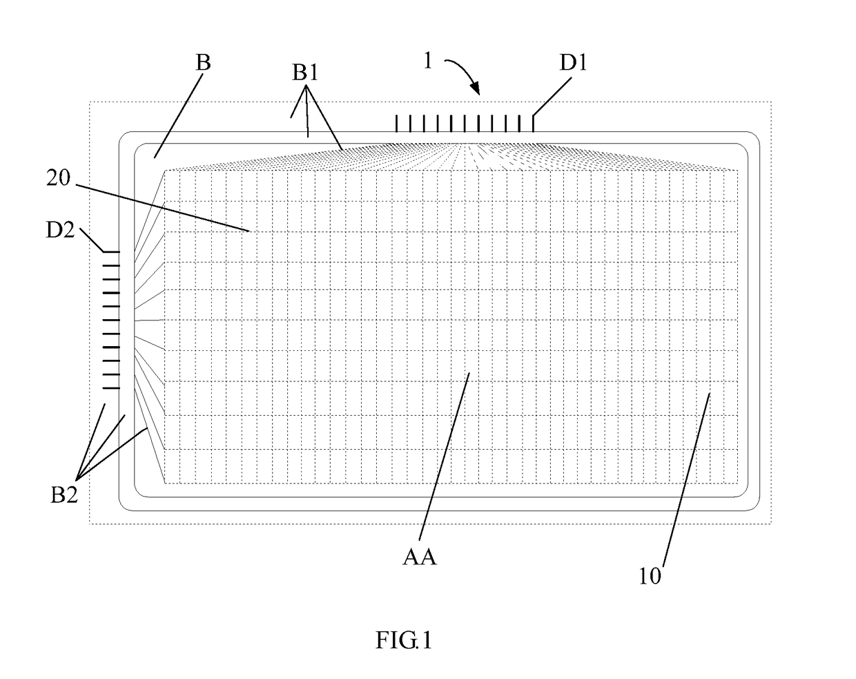
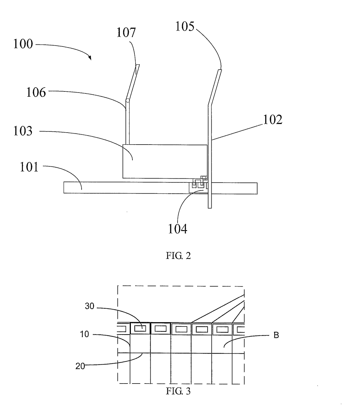
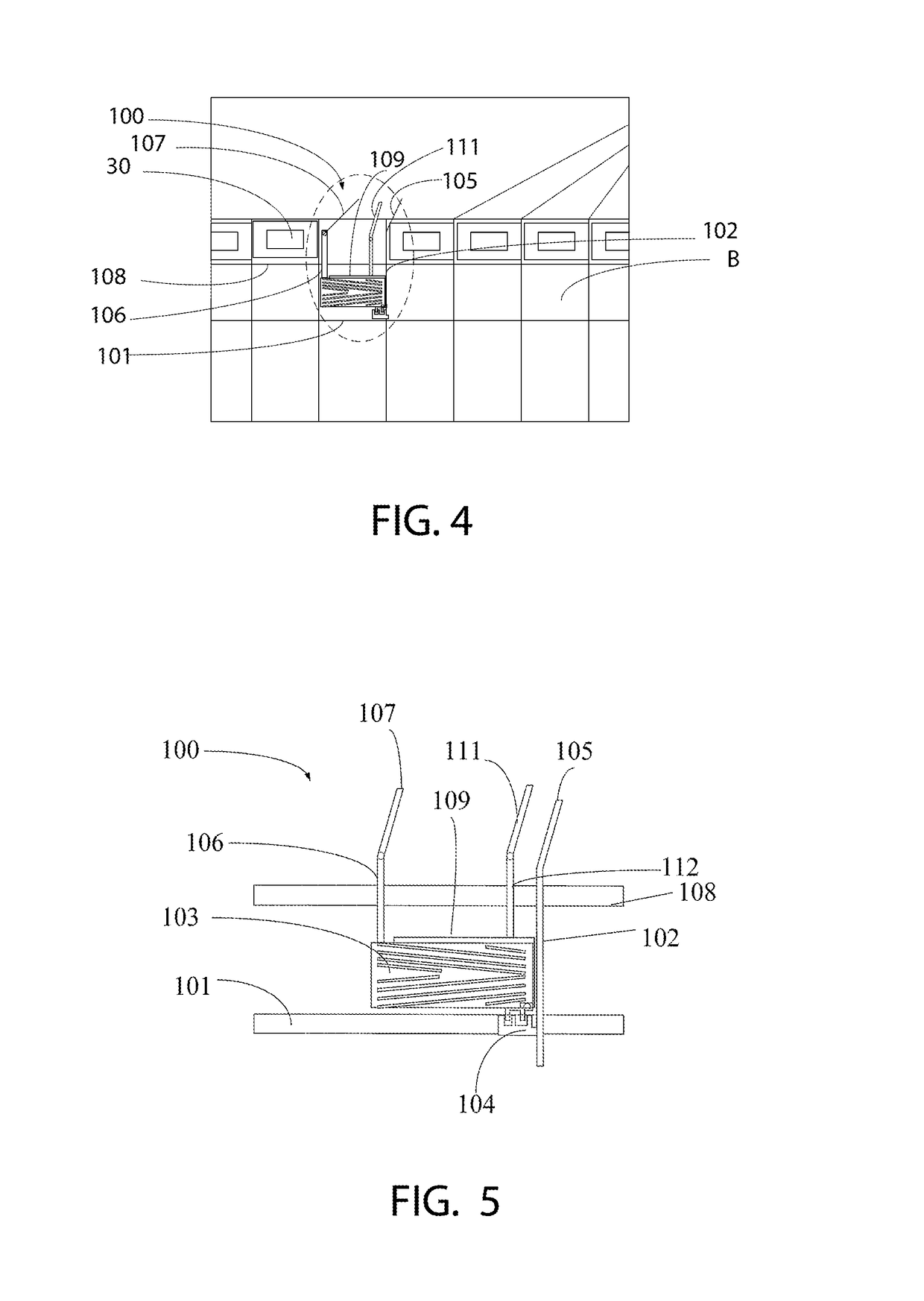
[0028]As to the failing of testing TFT performance as well as properties such as capacitance in the array substrate after the liquid crystal cell is formed in the prior art, an embodiment of the present invention provides an array substrate capable of testing TFT performance as well as properties such as capacitance of the array substrate without damage to the array substrate.

[0029]In embodiments of the present invention, a test unit is arranged in a peripheral circuit region on the array substrate, so as to effectively avoiding the failing of testing internal TFT performance as well as properties such as capacitance after the display panel is cell-assembled i...


PUM

PropertyMeasurementUnit
shapeaaaaaaaaaa
transparent conductiveaaaaaaaaaa
transparentaaaaaaaaaa

Abstract

An array substrate and a display device are provided. The array substrate includes a display region and a peripheral circuit region, wherein a first gate line, a first data line and a pixel region are arranged in the display region; the pixel region includes a first pixel electrode and a thin film transistor, and the thin film transistor includes a first gate electrode, a first source electrode and a first drain electrode; the peripheral circuit region is provided with at least one test unit including: a second gate line; a second data line; a second testing pixel electrode; and a second testing thin film transistor. The second testing thin film transistor includes a second gate electrode, a second source electrode and a second drain electrode, wherein the second gate electrode, the second source electrode and the second drain electrode are provided with test ports exposed outside.

Description

CROSS REFERENCE TO RELATED APPLICATIONS[0001]This application is the National Stage of PCT / CN2013 / 088998 filed on Dec. 10, 2013, which claims priority under 35 U.S.C. § 119 of Chinese Application No. 201310157333.0 filed on Apr. 28, 2013, the disclosure of which is incorporated by reference.TECHNICAL FIELD[0002]Embodiments of the invention relate to array substrate and display device.BACKGROUND[0003]Main body structure of a thin film transistor liquid crystal display (TFT-LCD) comprises an array substrate, a backlight and a drive circuit board.[0004]The array substrate of the TFT-LCD is of a layered structure formed by arranging a gate line, a gate insulating layer, an active layer, a source electrode, a drain electrode, a data line, a passivation layer and a pixel electrode on a transparent glass substrate, and is divided into a display region and a peripheral circuit region located in a periphery of the display region, wherein the peripheral circuit region is used for setting a da...

Claims


Application Information

Patent Timeline
Patent Type & Authority Patents(United States)
IPC IPC(8): H01L21/66G02F1/1362G02F1/1368H01L27/12
CPCH01L22/30G02F1/1362G02F1/136286H01L27/124G02F1/1368G02F2001/136254G02F1/136254
Inventor ZHANG, MINGMAO, GUOQIHAO, ZHAOHUIYOON, WOONG SUN
Owner BOE TECH GRP CO LTD
Why Eureka
Try Eureka