
Method of calibrating a nanometrology instrument

a nanometrology and instrument technology, applied in the direction of instruments, scanning probe techniques, etc., can solve the problems of increasing the size, weight and assembly costs of optical systems, adding costs, and challenging fabrication

Active Publication Date: 2019-11-12
THE UNITED STATES OF AMERICA AS REPRESENTED BY THE SECRETARY OF THE NAVY
View PDF10 Cites 0 Cited by
  • Summary
  • Abstract
  • Description
  • Claims
  • Application Information

AI Technical Summary

Problems solved by technology

The requirement of holding imaging optics and dispersive optics in precise alignments adds substantially to the size, weight, and assembly costs of optical systems.
Required tolerances for cavity length can be of nanometer order, making fabrication challenging.
Because each micro-fabrication step is time consuming and adds costs, minimizing the amount of fabrication steps is desired.
The resulting fabrication of a 1,000 level structure by digital etching is quite an effort.
However, measuring step speed on AFM images proves difficult due to spatial uncertainties associated with the electronics and mechanics of AFM.
A common problem for sequential AFM imaging is the thermal drift of piezos that causes the scanner to move away from the original field of view.
It is generally not difficult to obtain accurate XY calibration references.
It is, however, much more difficult to obtain accurate Z-axis results.
It is difficult to control Z piezo dynamics because, during scanning the X- and Y-axes move at a constant rate whiles the Z axis does not.
Due to the high cost of producing calibration standards, the microscope is often calibrated at only one height.
However, if the relationship between the measured Z height and the actual Z height is not linear, then the height measurements will not be correct.

Method used


Image

  • Method of calibrating a nanometrology instrument
  • Method of calibrating a nanometrology instrument
  • Method of calibrating a nanometrology instrument

Examples


Embodiment Construction

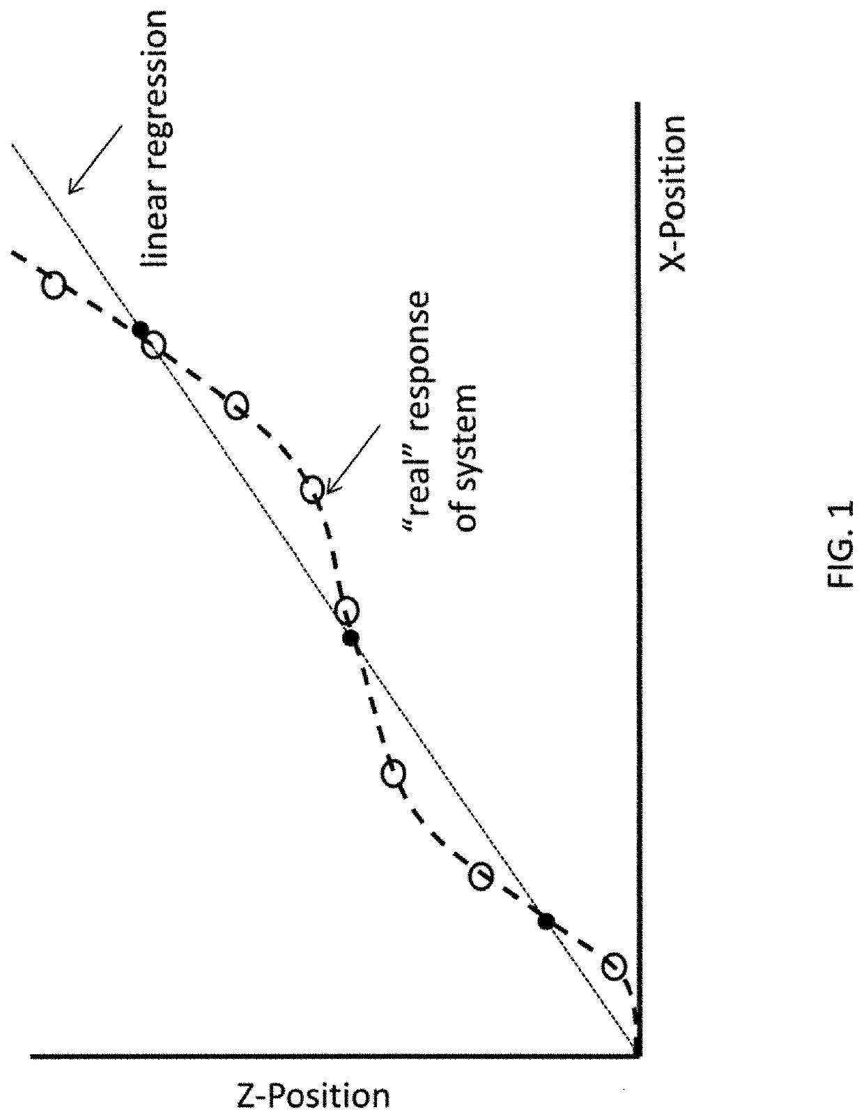
[0022]Referring by way of illustration to FIG. 1, Applicants recognized the difficulty of calibrating a nanometrology instrument. In FIG. 1, the X-position axis represents a horizontal dimension, and the Z-position axis represents a vertical or height dimension. The dotted line in FIG. 1 represents a theoretical system response from a nanometrology instrument. The theoretical system response is a linear regression line. The dashed line in FIG. 1 represents a more representative “real” response of the nanometrology instrument. Comparing the theoretical system response with the real response of the nanometrology instrument, Applicants recognized that the real response was not a linear regression. Applicants realized that if the nanometrology instrument were to be calibrated based on a few measured heights, e.g., as represented by black dots, the user calibrating the nanometrology instrument would assume a perfect, linear fit. However, as can be seen in FIG. 1, the real response includ...


PUM


Abstract

A method of calibrating a topography metrology instrument using a calibration reference, which includes a substrate and a plurality of bi-layer stacks. Each bi-layer stack includes a plurality of bi-layer steps. At least one bi-layer step of the plurality of bi-layer steps includes two materials. The at least one bi-layer step of the plurality of bi-layer steps includes an etch stop layer and a bulk layer. The calibration reference includes a calibration reference step profile includes a plurality of predetermined bi-layer stack heights. The calibration reference step profile and the predetermined bi-layer stack heights are measured using a topography metrology instrument. The topography metrology instrument is calibrated based on the measured calibration reference step profile and the measured bi-layer stack heights.

Description

CROSS-REFERENCE TO RELATED APPLICATIONS[0001]This application claims priority to U.S. Provisional Patent Application Ser. No. 62 / 057,333, entitled “CALIBRATION REFERENCE TO NANOMETROLOGY,” to Christophersen et al., which was filed on 30 Sep. 2014 and is incorporated herein by reference. This application further is a continuation-in-part application to, and claims priority to, U.S. patent application Ser. No. 14 / 269,292, entitled “FABRICATION METHOD FOR DIGITAL ETCHING OF NANOMETER-SCALE LEVEL STRUCTURES,” to Boudreau et al., which was filed on 5 May 2013 and is incorporated herein by reference.BACKGROUND OF THE INVENTION[0002]Field of the Invention[0003]This invention relates in general to a method for calibrating a scanner, and in particular to a method of calibrating a nanometrology device.[0004]Description of the Related Art[0005]Conventional spectrometers typically use dispersive elements to separate light into its spectral components, requiring space and precise alignment of de...

Claims


Application Information

Patent Timeline
Patent Type & Authority Patents(United States)
IPC IPC(8): G01Q40/02
CPCG01Q40/02
Inventor CHRISTOPHERSEN, MARCPHLIPS, BERNARD F.BOUDREAU, ANDREW J.YETZBACHER, MICHAEL K.
Owner THE UNITED STATES OF AMERICA AS REPRESENTED BY THE SECRETARY OF THE NAVY
Learn More