Light emitting device including variable transmission film to control intensity and pattern
a light emitting device and transmission film technology, applied in the direction of semiconductor devices for light sources, lighting elements, lighting and heating apparatus, etc., can solve problems such as inconsistency in light color
- Summary
- Abstract
- Description
- Claims
- Application Information
AI Technical Summary
Benefits of technology
Problems solved by technology
Method used
Image

Examples
second embodiment
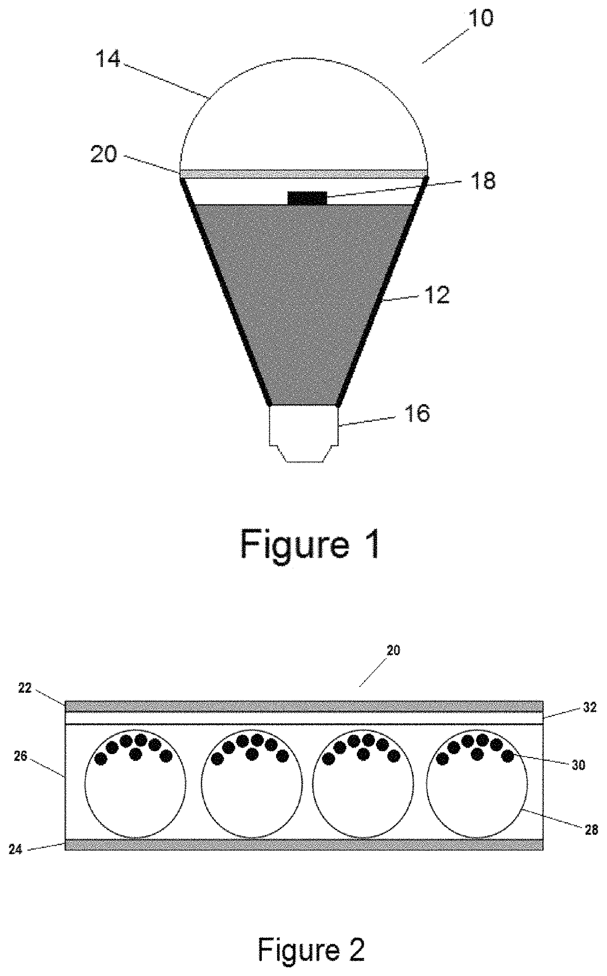
[0034]In the present invention, the cover 14 in the device 10 illustrated in FIG. 1 may be transparent, and the light source 18 and / or housing 12 configured to focus the light into a narrow beam, such as a task light. The charged particles 30 in the encapsulated electrophoretic medium 26 may then comprise white, diffusive particles. When the variable transmissive film 20 is in an open state, such as the light transmissive state illustrated in FIG. 3, the device 10 will operate as a task light. However, when the variable transmissive film 20 is switched to a closed state, such as the opaque state illustrated in FIG. 2, the white charged particles 30 will diffuse the light emitted by the light source 18, thereby providing a “frosted” cover. This provides a method of switching between task lighting and ambient lighting without the need for any mechanical components for re-focusing the light emitted from the light source.
third embodiment
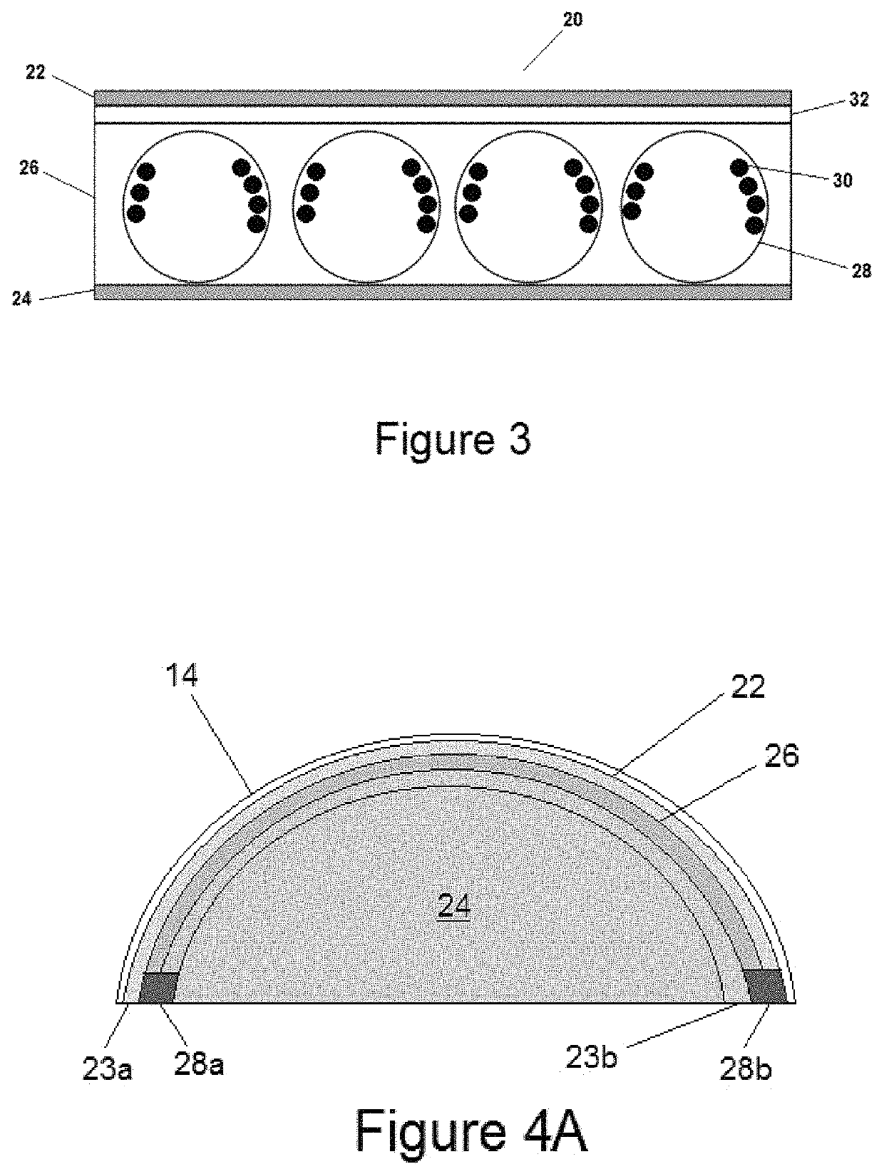
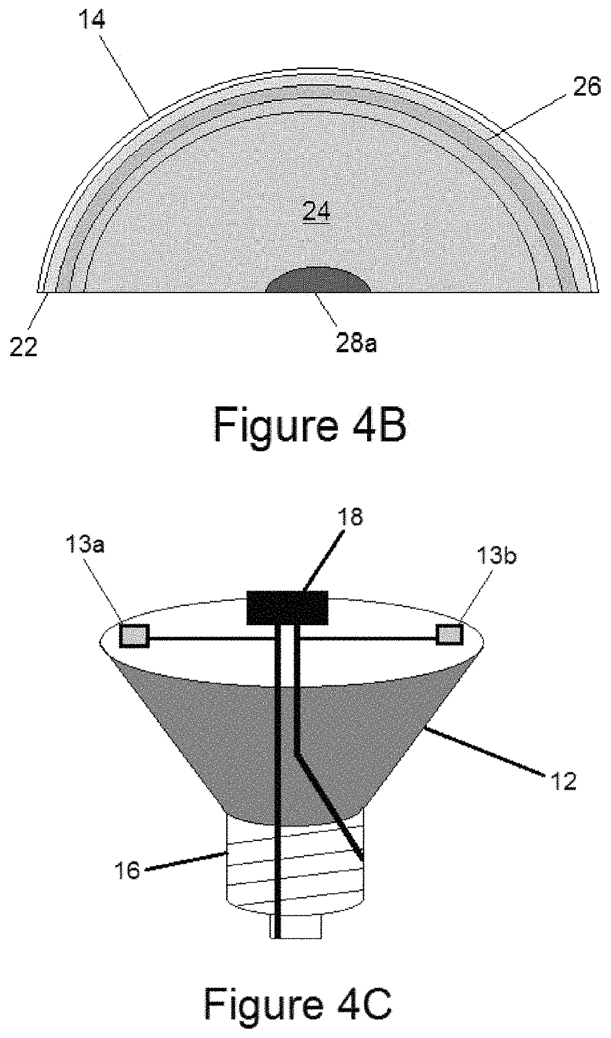
[0035]In the present invention, the light emitting device may be modified, such that the variable transmissive film and the cover of the light emitting device are combined into a single component. For example, referring to FIGS. 4A and 4B, the cover 14 may provide a light transmissive curved substrate on which a first layer of conductive material is applied to an inner surface of the cover 14 to provide a first electrode layer 22, a layer of electrophoretic medium 26 is applied over the first electrode layer 22, and a second layer of conductive material is applied over the layer of electrophoretic medium 26 to form a second electrode layer 24. Alternatively, the successive layer may be applied in order to the outside surface of the cover 14. Also an optional protective layer may be applied over the top electrode layer.
[0036]In order to separate the first and second electrode layers 22, 24 to prevent an electrical short that may circumvent the application of an electric field to the ...
PUM
| Property | Measurement | Unit |
|---|---|---|
| frequency | aaaaa | aaaaa |
| size | aaaaa | aaaaa |
| dielectric constant | aaaaa | aaaaa |
Abstract
Description
Claims
Application Information