Supercharge Your Innovation With Domain-Expert AI Agents!

Pixel circuit, display device and detecting method

a display device and circuit technology, applied in the field of circuits, a display device and a display device, can solve problems such as image non-uniformity and led driving circuit caused by problems

Active Publication Date: 2021-11-02
INNOLUX CORP
View PDF7 Cites 5 Cited by
  • Summary
  • Abstract
  • Description
  • Claims
  • Application Information

AI Technical Summary

Benefits of technology

The patent describes a pixel circuit, a display device, and a detecting method for monitoring current and voltage in a pixel circuit. The pixel circuit includes a first transistor, a second transistor, a third transistor, and a light emitting unit. By detecting the current of a specific node when the first transistor is turned off, the device can be used to display images or videos with improved accuracy and control. The technical effects of this patent include improved image and video quality, reduced power consumption, and increased control over pixel circuits.

Problems solved by technology

Image non-uniformity which caused by an LED driving circuit has been a problem.
The image non-uniformity is caused by TFT variation in manufacturing the LED display device, and further leads to, for example, the mura effect.

Method used


Image

  • Pixel circuit, display device and detecting method
  • Pixel circuit, display device and detecting method
  • Pixel circuit, display device and detecting method

Examples


Embodiment Construction

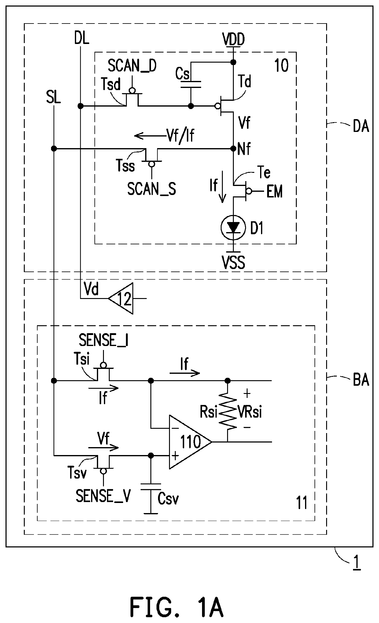
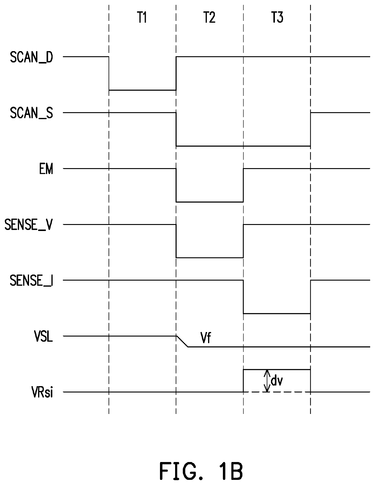
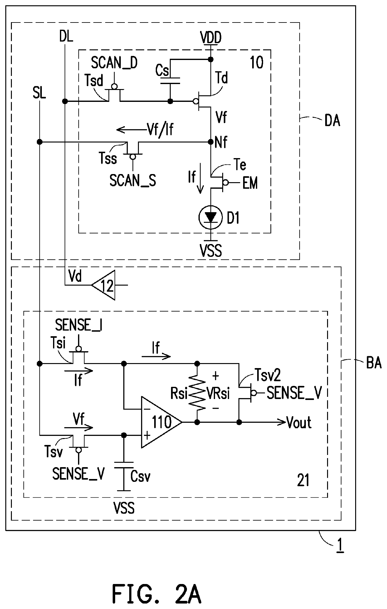
[0033]The following embodiments when read with the accompanying drawings are made to clearly exhibit the above-mentioned and other technical contents, features and / or effects of the present disclosure. Through the exposition by means of the specific embodiments, people would further understand the technical means and effects the present disclosure adopts to achieve the above-indicated objectives. Moreover, as the contents disclosed herein should be readily understood and can be implemented by a person skilled in the art, all equivalent changes or modifications which do not depart from the concept of the present disclosure should be encompassed by the appended claims.

[0034]Certain terms are used throughout the description and following claims to refer to particular components. As one skilled in the art will understand, electronic equipment manufacturers may refer to a component by different names. This document does not intend to distinguish between components that differ in name but...


PUM


Abstract

A pixel circuit is provided. The pixel circuit includes a first transistor, a second transistor, a third transistor, and a light emitting unit. The second transistor is coupled to the first transistor. The third transistor is coupled to the second transistor. The light emitting unit is coupled to the first transistor. When the first transistor is turned off, a current of a node between the third transistor and the first transistor is detected.

Description

BACKGROUND1. Technical Field[0001]The disclosure generally relates to a circuit, a device and a method, in particular, to a pixel circuit and a display device of a light-emitting diode (LED) and a detecting method.2. Description of Related Art[0002]Image non-uniformity which caused by an LED driving circuit has been a problem. The image non-uniformity is caused by TFT variation in manufacturing the LED display device, and further leads to, for example, the mura effect. Therefore, there is necessity to improve the above problem.SUMMARY[0003]Accordingly, the disclosure is directed to a pixel circuit, a display device and a detecting method that a current monitoring function and / or a voltage monitoring function are provided.[0004]The pixel circuit of the disclosure includes a first transistor, a second transistor, a third transistor, and a light emitting unit. The second transistor is coupled to the first transistor. The third transistor is coupled to the second transistor. The light e...

Claims


Application Information

Patent Timeline
IPC IPC(8): G09G3/00G09G3/32
CPCG09G3/006G09G3/32G09G2310/0267G09G2310/0275G09G2310/0291G09G2330/12G09G2320/029G09G3/3233G09G2310/0248G09G2320/0233
Inventor HASHIMOTO, KAZUYUKI
Owner INNOLUX CORP
Features
  • R&D
  • Intellectual Property
  • Life Sciences
  • Materials
  • Tech Scout
  • Unparalleled Data Quality
  • Higher Quality Content
  • 60% Fewer Hallucinations
Learn More