Display panel, manufacturing method of same, and tiled display panel

a technology of display panel and manufacturing method, applied in the field of display, can solve the problems of reducing display quality, increasing screen size, and increasing manufacturing difficulty and manufacturing cost per unit area, and achieve the effect of eliminating or reducing seams and being easy to separa

Active Publication Date: 2022-02-01
SHENZHEN CHINA STAR OPTOELECTRONICS SEMICON DISPLAY TECH CO LTD
View PDF12 Cites 2 Cited by
  • Summary
  • Abstract
  • Description
  • Claims
  • Application Information

AI Technical Summary

Benefits of technology

[0004]In view of this, the present disclosure aims to provide a bezel-free or narrow-bezel display panel and a manufacturing method of the same. Besides, the present disclosure also provides a tiled display panel which can eliminate or reduce seams.
[0053]A tiled display panel according to the present disclosure is formed by tiling the above-mentioned bezel-free display panel or narrow-bezel display panel. Seams can be narrowed to a size of one-pixel unit, so as to make the seams difficult to be recognized by naked eyes to users and obtain an effect of eliminating or reducing seams.
[0054]According to the manufacturing method of a display panel according to one embodiment of the present discourse, by disposing the fanout circuit and the fanout circuit base layer on the surface of the array substrate and forming through-holes in the fanout circuit base layer and etching the metallic sacrificial layer between the fanout circuit base layer and the array substrate via the though-holes, the fanout circuit base layer and the array substrate can be easily separated without a step of laser lift-off. When the bonding of a driver chip is completed and the array substrate outside the bezel region is already cut off, the fanout circuit and the flexible fanout circuit base layer can be bent to a back of the display substrate. An area of the bezel region of the display panel can be narrowed, so as to obtain an effect of bezel-free and narrow-bezel.

Problems solved by technology

As for displays, such as liquid crystal displays (LCDs), organic light-emitting diode displays (OLEDs), and light emitting diode displays (LEDs), the larger the screen size, the higher the manufacturing difficulty and the manufacturing cost per unit area.
The existence of bezels of the small or medium-sized displays will lead to presence of bar shaped seams in display areas of tiled display panels, thus lowering display quality.

Method used


Image

  • Display panel, manufacturing method of same, and tiled display panel
  • Display panel, manufacturing method of same, and tiled display panel
  • Display panel, manufacturing method of same, and tiled display panel

Examples


Embodiment Construction

[0061]The present disclosure is further described in detail below with reference to the accompanying drawings and embodiments. Obviously, the following described embodiments are only part of the present disclosure but not all. A person having ordinary skill in the art may obtain other embodiments based on the embodiments provided in the present disclosure without making any creative effort, which all belong to the scope of the present disclosure.

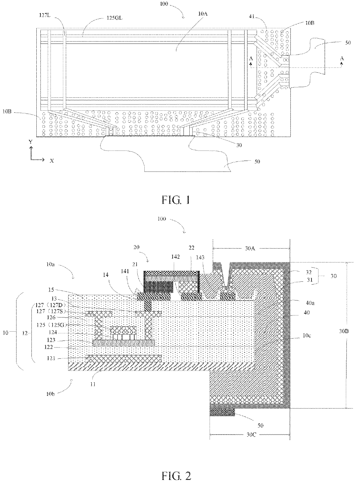
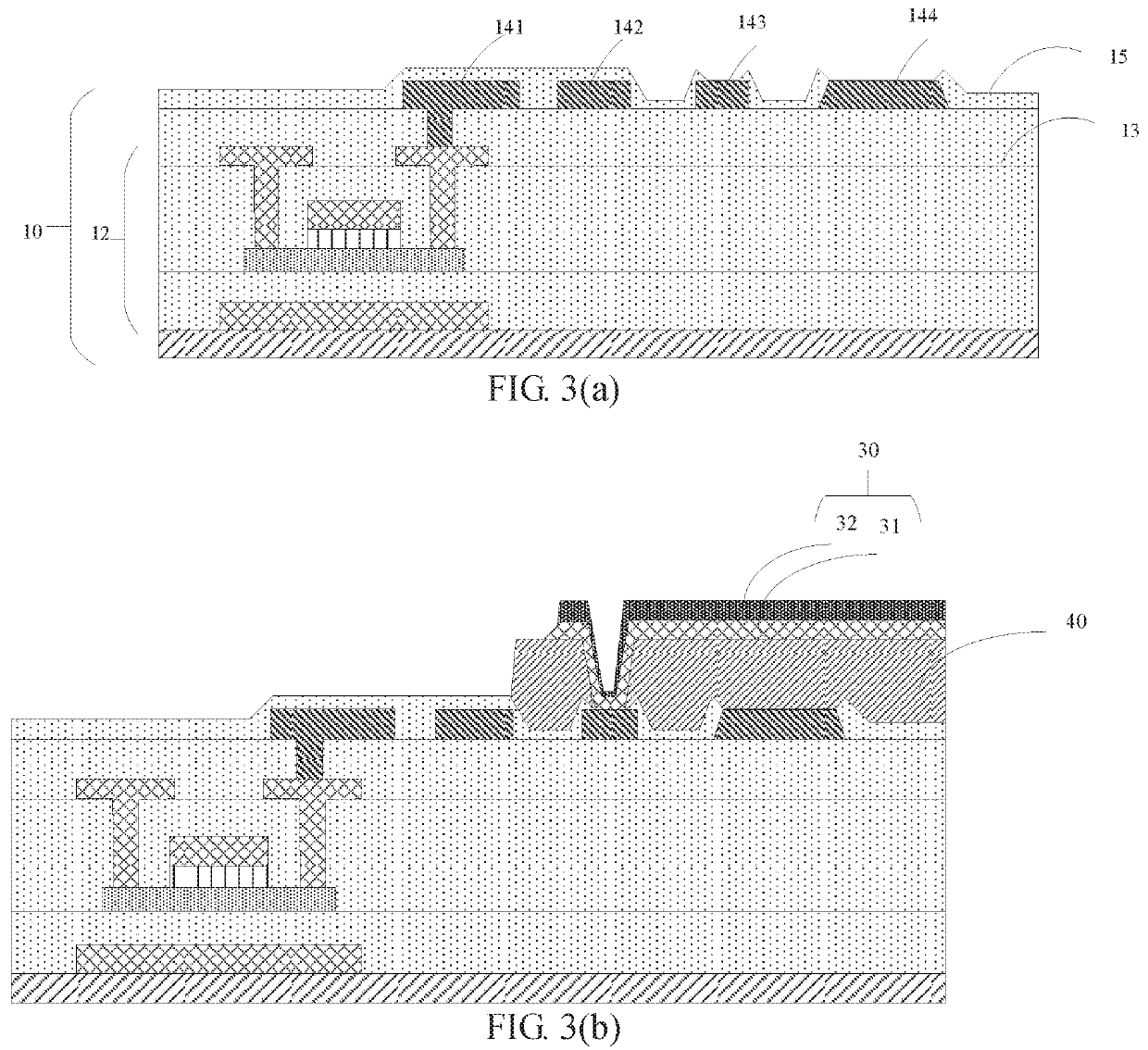
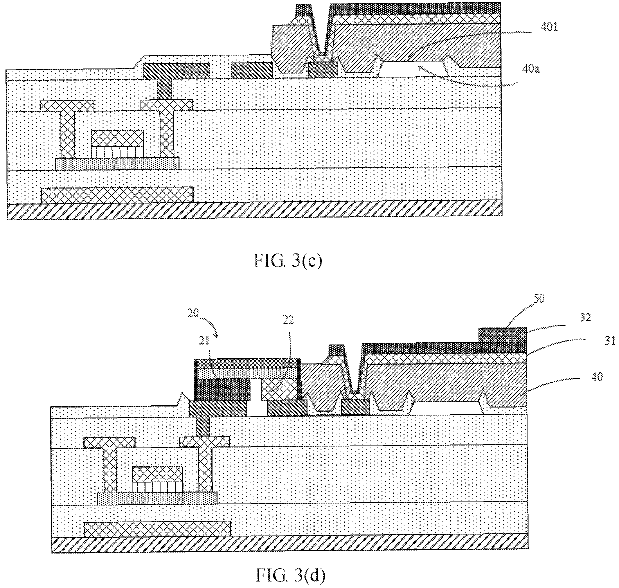
[0062]Please refer to FIG. 1 and FIG. 2, a display panel 100 according to one embodiment of the present disclosure comprises an array substrate 10, a light-emitting layer 20, a fanout circuit 30, a fanout circuit base layer 40, and a driver chip 50. The array substrate 10 comprises a display area 10A and a trace area 10B located around the display area 10A. The light-emitting layer 20 is located on the display area 10A and the light-emitting layer 20 is electrically connected to a first side 10a of the array substrate 10. The fanout circuit ...


PUM

PropertyMeasurementUnit
areaaaaaaaaaaa
sizeaaaaaaaaaa
flexibleaaaaaaaaaa

Abstract

A display panel comprises: an array substrate comprising a display area and a trace area located around the display area; a light-emitting layer located in the display area and electrically connected to a first side of the array substrate; a fanout circuit located in the trace area; a fanout circuit base layer disposed between the fanout circuit and the array substrate; and a driver chip located at a second side of the array substrate; wherein the fanout circuit and the fanout circuit base layer are bent from the first side to the second side along a sidewall of the array substrate, the fanout circuit is electrically connected to the array substrate at the first side, and the fanout circuit is electrically connected to the driver chip at the second side.

Description

RELATED APPLICATIONS[0001]This application is a National Phase of PCT Patent Application No. PCT / CN2019 / 118880 having International filing date of Nov. 15, 2019, which claims the benefit of priority of Chinese Patent Application No. 201911042705.9 filed on Oct. 30, 2019. The contents of the above applications are all incorporated by reference as if fully set forth herein in their entirety.FIELD AND BACKGROUND OF THE INVENTION[0002]The present disclosure relates to the display field, and particularly relates to a display panel, a manufacturing method of same, and a tiled display panel.[0003]In the display field, bezel-free displays or narrow-bezel displays have gradually become mainstream. As for displays, such as liquid crystal displays (LCDs), organic light-emitting diode displays (OLEDs), and light emitting diode displays (LEDs), the larger the screen size, the higher the manufacturing difficulty and the manufacturing cost per unit area. Therefore, large-size displays are usually ...

Claims


Application Information

Patent Timeline
Patent Type & Authority Patents(United States)
IPC IPC(8): H01L27/15H01L33/62G09F9/33H01L33/00H01L33/48
CPCH01L27/156G09F9/33H01L33/005H01L33/486H01L33/62G09G2360/04H01L2933/0066H01L25/167
Inventor LU, MACAI
Owner SHENZHEN CHINA STAR OPTOELECTRONICS SEMICON DISPLAY TECH CO LTD
Why Eureka
Try Eureka