Optoelectronic assembly and method for producing an optoelectronic assembly

a technology of optoelectronic components and assemblies, which is applied in the direction of photovoltaic energy generation, electrical apparatus, and semiconductor devices, can solve the problems of voltage rise and luminance drop, and achieve the effect of simple and/or compact manner, prolonging the lifetime of the corresponding organic optoelectronic component, and intensifying the encapsulation

Active Publication Date: 2022-06-28
PICTIVA DISPLAY INT LTD
View PDF18 Cites 0 Cited by
  • Summary
  • Abstract
  • Description
  • Claims
  • Application Information

AI Technical Summary

Benefits of technology

[0008]The operating lifetime of the OLED at a predefined ambient temperature may be increased by optimizing the organic layer stack and the encapsulation. Furthermore, attempts are made to minimize the source term P_heat by means of particularly efficient OLEDs. This may have the effect that the OLED is constructed in a particularly complex fashion and / or is producible with a particularly high outlay.
[0037]In accordance with one development, the radiation cooler includes a layer structure including a plurality of different layers, wherein the layers have different refractive indices and at least partly different layer thicknesses, wherein in a first thickness region of the layer structure layers are formed which have thicknesses which are greater than the thicknesses of layers in a second thickness region. The layers having the different refractive indices and the different thickness regions have the effect that the radiation cooler cools down relative to the ambient temperature even under direct insolation.

Problems solved by technology

In this case, aging as a result of the operation of an OLED at a constant current density is manifested by a rise in voltage and a fall in luminance.

Method used


Image

  • Optoelectronic assembly and method for producing an optoelectronic assembly
  • Optoelectronic assembly and method for producing an optoelectronic assembly
  • Optoelectronic assembly and method for producing an optoelectronic assembly

Examples


Embodiment Construction

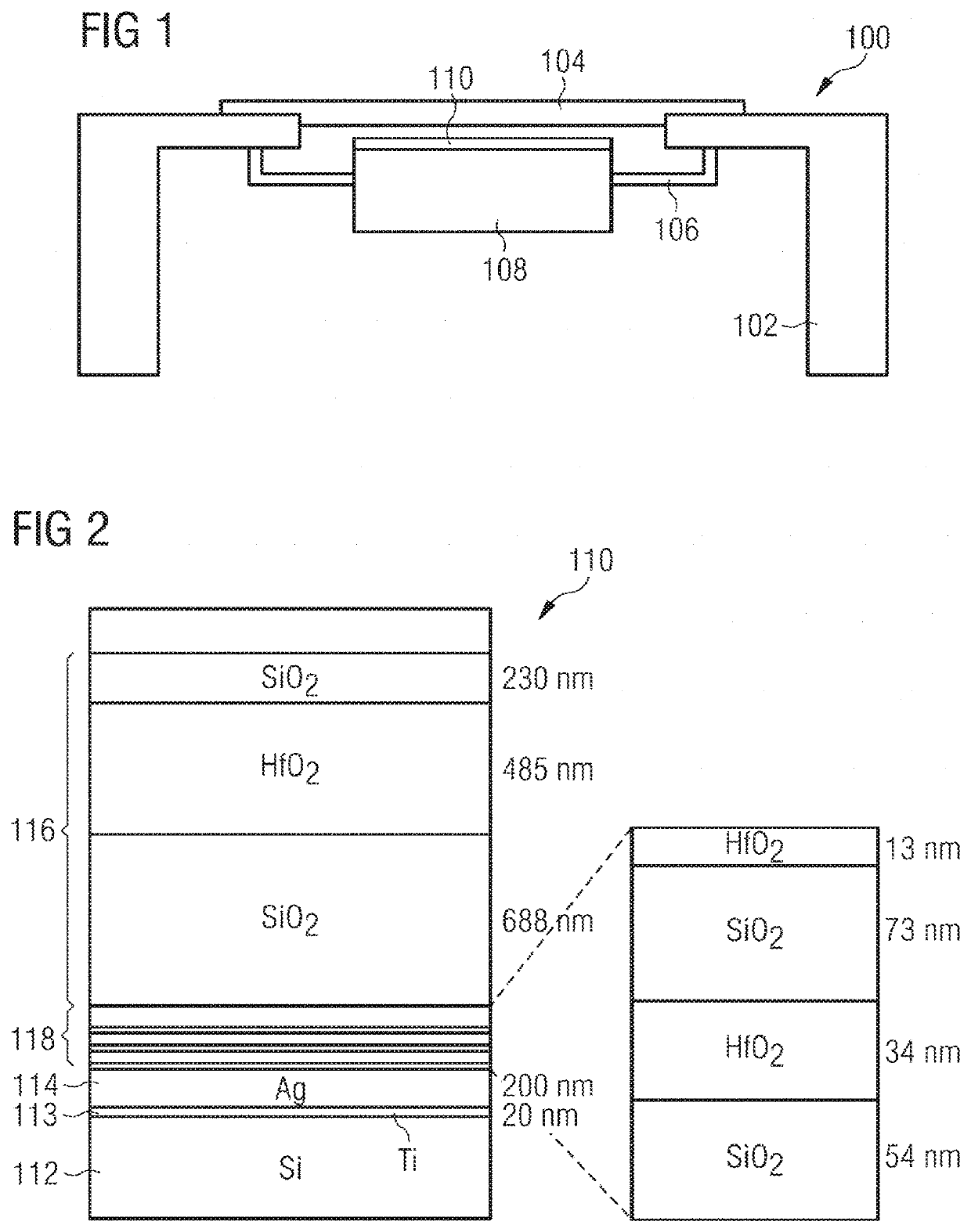
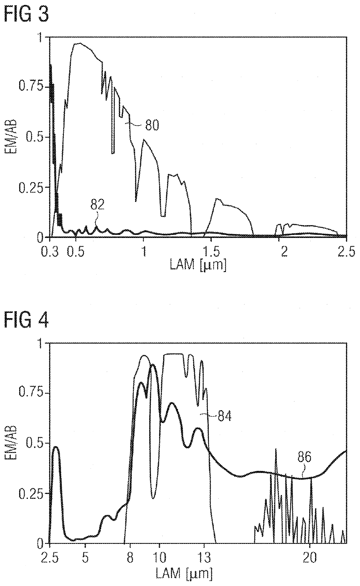
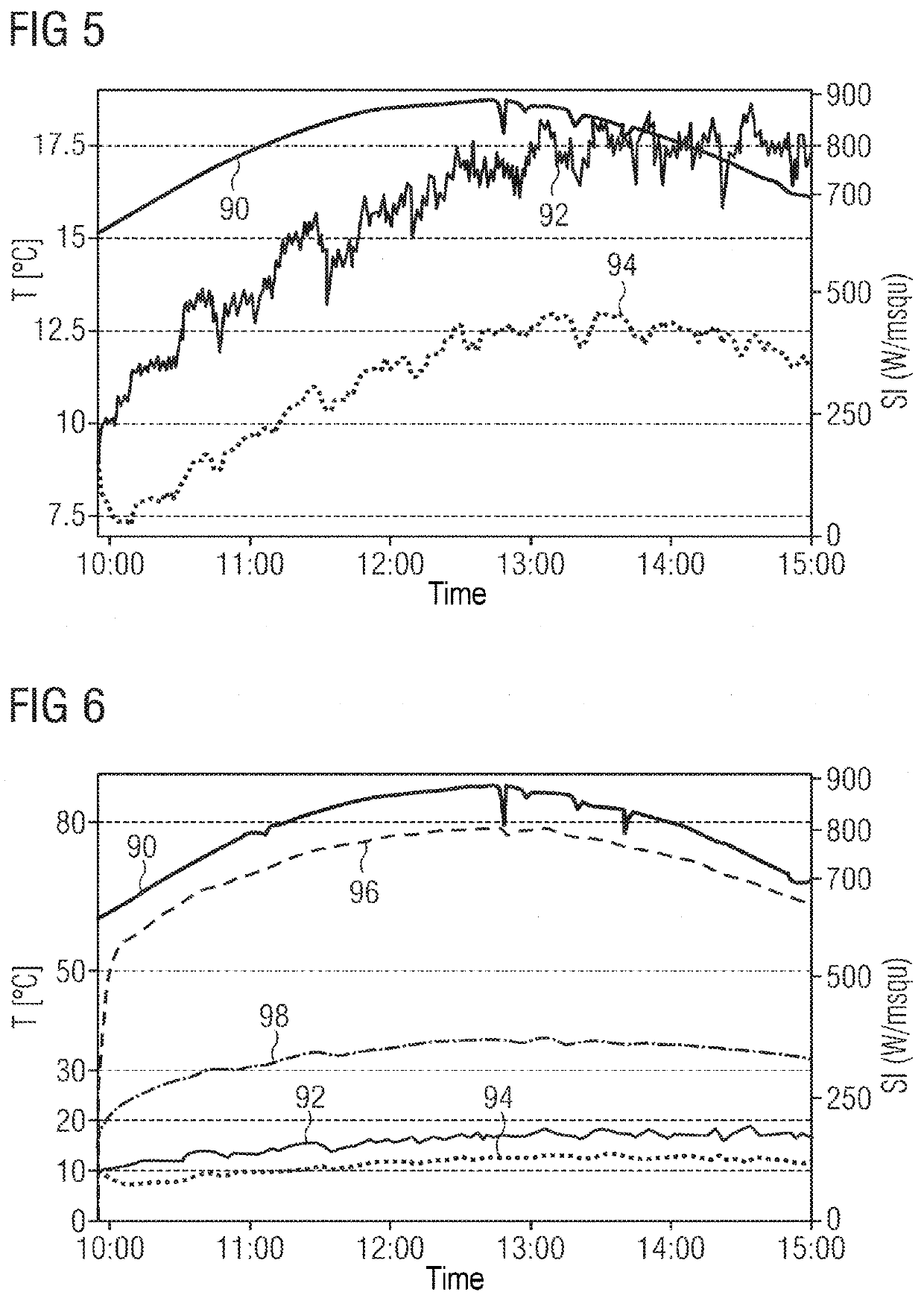
[0060]In the following detailed description, reference is made to the accompanying drawings, which form part of this description and show for illustration purposes specific embodiments in which the invention may be implemented. Since component parts of embodiments may be positioned in a number of different orientations, the direction terminology serves for illustration and is not restrictive in any way whatsoever. It goes without saying that other embodiments may be used and structural or logical changes may be made, without departing from the scope of protection of the present disclosure. It goes without saying that the features of the various embodiments described herein may be combined with one another, unless specifically indicated otherwise. Therefore, the following detailed description should not be interpreted in a restrictive sense, and the scope of protection of the present disclosure is defined by the appended claims. In the figures, identical or similar elements are provi...


PUM

PropertyMeasurementUnit
thicknessaaaaaaaaaa
thicknessaaaaaaaaaa
temperatureaaaaaaaaaa

Abstract

An optoelectronic assembly comprising an optoelectronic component, which comprises a specularly reflective surface and comprising a radiation cooler in direct physical contact with the optoelectronic component. The radiation cooler is arranged above the specularly reflective surface.

Description

CROSS-REFERENCE TO RELATED APPLICATIONS[0001]The present application is a continuation of U.S. patent application Ser. No. 16 / 070,534, filed Jul. 17, 2018, allowed, which application is a national stage entry according to 35 U.S.C. § 371 of PCT application No.: PCT / EP2017 / 051993 filed on Jan. 31, 2017, which claims priority from German Patent Application Serial No.: 10 2016 101 788.4 which was filed Feb. 2, 2016, and is incorporated herein by reference in its entirety and for all purposes.TECHNICAL FIELD[0002]The disclosure relates to an optoelectronic assembly and to a method for producing an optoelectronic assembly.SUMMARY OF THE INVENTION[0003]An optoelectronic assembly may include one, two or more optoelectronic components. An optoelectronic component may be an electromagnetic radiation emitting component or an electromagnetic radiation absorbing component. An electromagnetic radiation absorbing component may be a solar cell, as a non-limiting example. An electromagnetic radiati...

Claims


Application Information

Patent Timeline
Patent Type & Authority Patents(United States)
IPC IPC(8): H01L51/52
CPCH01L51/529H01L51/5237H10K50/87Y02E10/549H10K50/84
Inventor PENTLEHNER, DOMINIKBAISL, RICHARD
Owner PICTIVA DISPLAY INT LTD
Why Eureka
Try Eureka