
Eureka
For R&D, Eureka makes reading and utilizing patents & technical documents easy.
Eureka AIR
Designed for self-driven R&D workflows. Generate viable solutions, solve complex R&D challenges, empower your innovation with AI.

Eureka Materials
Designed for material experts only. Revolutionize your material R&D, from search, analyze, to developing new materials.

TechResearch
Generate reliable direction feasibility study reports for your R&D in just a few steps.

TechSeek
Discover and master advanced knowledge NOW. Basics, ideas, possibilities, all at once.

TechMind
As an expert in R&D Theories, TechMind can generates customized viable solutions instantly.

TechRisk
Analyze your overall solution with one click, know your potential R&D risks in advance.

TechMonitor
Get weekly tech updates, stay abreast of the latest tech innovations and key insights.
IC socket and method of mounting IC package
- Summary
- Abstract
- Description
- Claims
- Application Information
AI Technical Summary
Problems solved by technology
Method used
Image

Examples
embodiment 2
[0062] FIG. 10 and FIG. 11 are schematic diagrams showing a process of mounting an IC package when the IC package of the present invention is of a ball grid array type, with FIG. 10 representing a first step and FIG. 11 representing a second step.
[0063] As shown in FIG. 10 and FIG. 11, the IC package mounting method according to the second embodiment of the present invention concerns a ball grid array type of IC package.
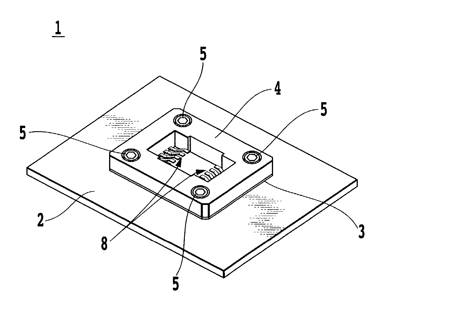
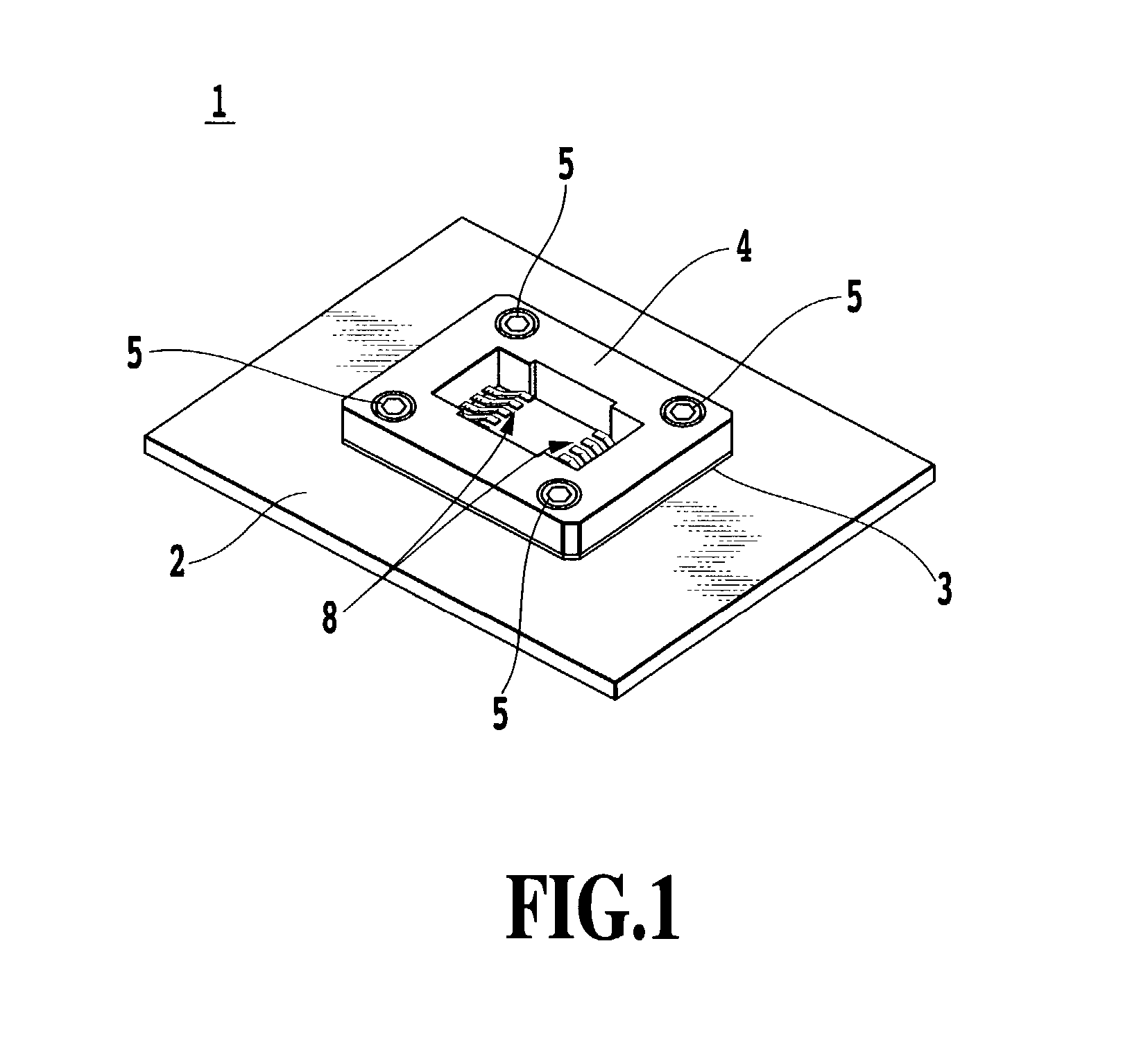
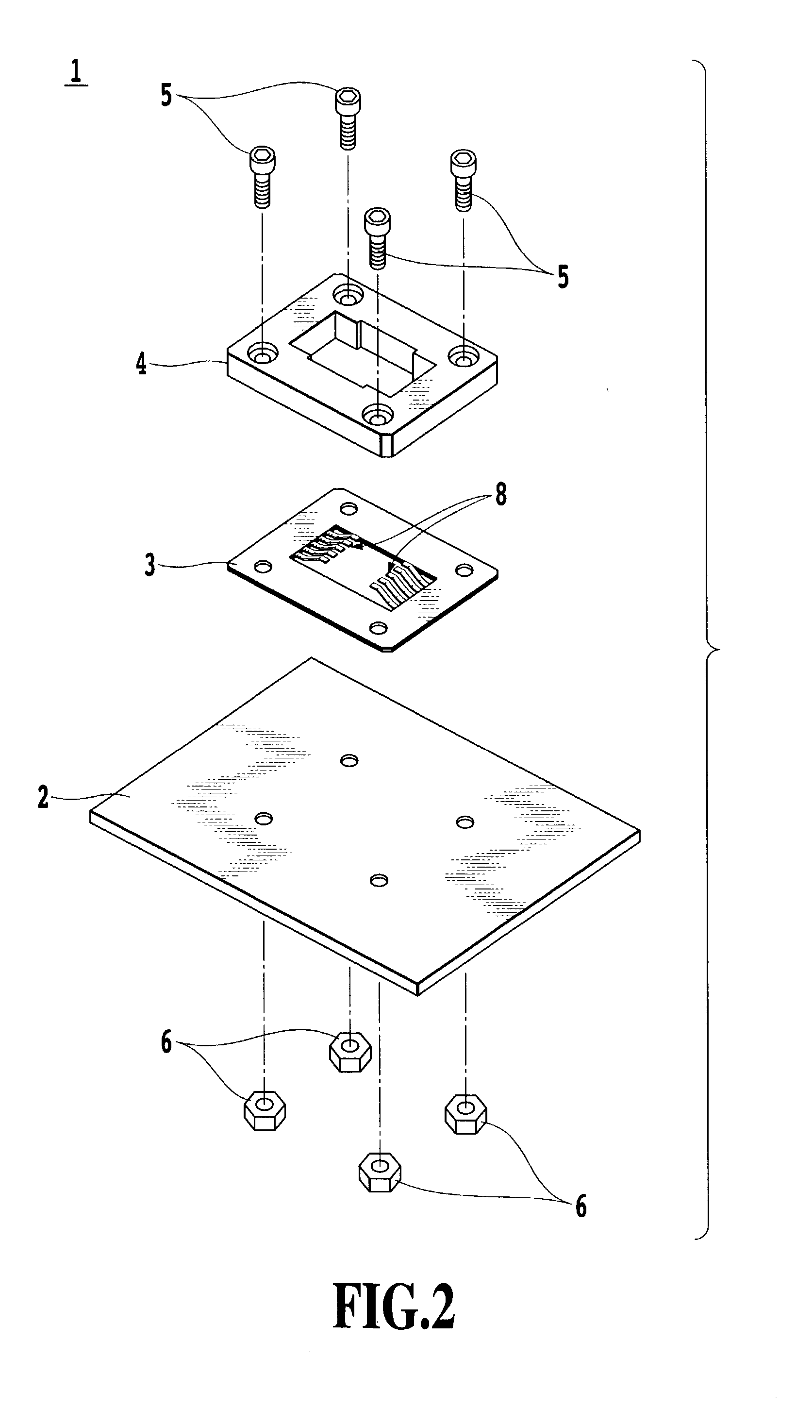
[0064] As shown in FIG. 10, in the first step of the present invention, a contact sheet 12 for a ball grid array type of IC package 15 is fastened to a carrier 11 concurrently used as a socket frame with a plurality of screws 13. The carrier 11 has a hole 17 at almost the center in which to mount the IC package 15 and also two holes 18 located diagonally of the carrier with the hole 17 therebetween, in which mounting legs 19 of a pusher 16 are to be inserted. The pusher 16 has a raised press portion 20 at almost the center of underside thereof which is to be fitted i...
embodiment 3
[0068] FIG. 12 and FIG. 13 are schematic diagrams showing another IC package mounting method of the present invention when the IC package is of a quad flat plate type, with FIG. 12 representing a first step and FIG. 13 representing a second step. The IC package mounting method of this embodiment differs from that of Embodiment 2 in that the IC package is of a quad flat plate type. Thus, a contact sheet used, too, is of a quad flat plate type.
[0069] In the first step of the present invention, as shown in FIG. 12, a contact sheet 22 for an IC package 25 of a quad flat plate type is fastened to a carrier 21 concurrently used as a socket frame with a plurality of screws 23. The carrier 21 has a hole 27 at almost the center for mounting the IC package 25 and also two holes 28 located diagonally of the carrier with the hole 27 therebetween, in which mounting legs 29 of a pusher 26 are to be inserted. The pusher 26 has a raised press portion 30 at almost the center of the underside surface...
PUM
 Abstract
Description
Claims
Application Information
 - R&D Engineer
- R&D Manager
- IP Professional
- Industry Leading Data Capabilities
- Powerful AI technology
- Patent DNA Extraction
Browse by: Latest US Patents, China's latest patents, Technical Efficacy Thesaurus, Application Domain, Technology Topic, Popular Technical Reports.
© 2024 PatSnap. All rights reserved.Legal|Privacy policy|Modern Slavery Act Transparency Statement|Sitemap|About US| Contact US: help@patsnap.com