Variable impedance circuit

a technology of impedance circuit and resistor, which is applied in the direction of logic circuit coupling/interface arrangement, impedence matching network, instruments, etc., can solve the problems of mos transistor or resistor resistance deviating from the design resistance, degrading the accuracy of the resistance obtained therein, and i/o circuit signal wave degradation

Inactive Publication Date: 2002-12-12
RENESAS ELECTRONICS CORP
View PDF0 Cites 16 Cited by
  • Summary
  • Abstract
  • Description
  • Claims
  • Application Information

AI Technical Summary

Problems solved by technology

Although the impedance matching scheme generally uses MOS transistors or resistors, there is a problem in that the resistances of the MOS transistors or resistors deviate from the design resistances due to characteristic variances associated therewith.
This fact may degrade the accuracy of the resistance obtained therein as will be detailed hereinafter.
In such a case, degradation of the signal wave may occur in the I / O circuit due to the mismatching of the impedance.

Method used


Image

  • Variable impedance circuit
  • Variable impedance circuit
  • Variable impedance circuit

Examples


Embodiment Construction

[0028] Now, the present invention is more specifically described with reference to accompanying drawings, wherein similar constituent elements are designated by similar reference numerals.

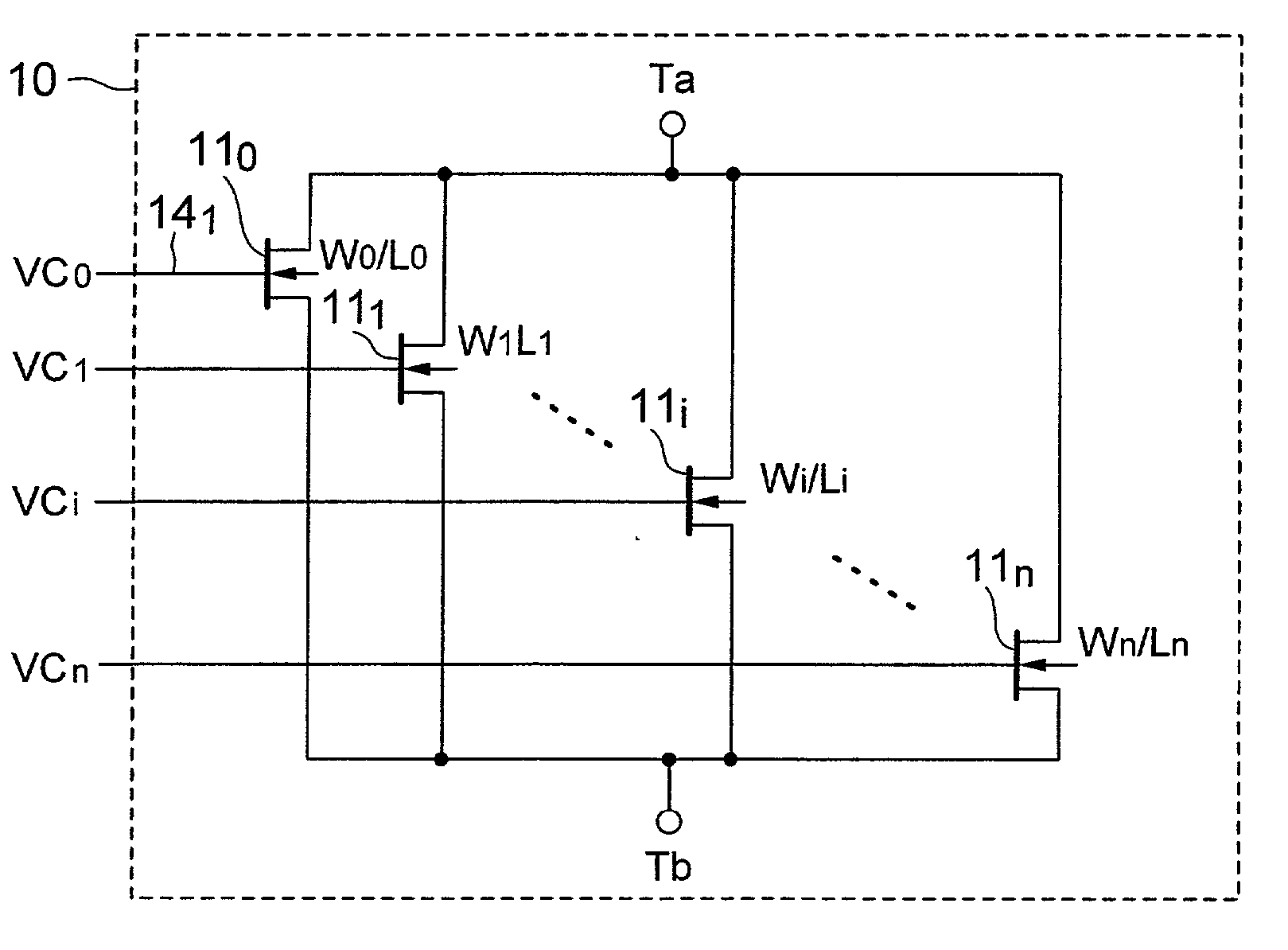
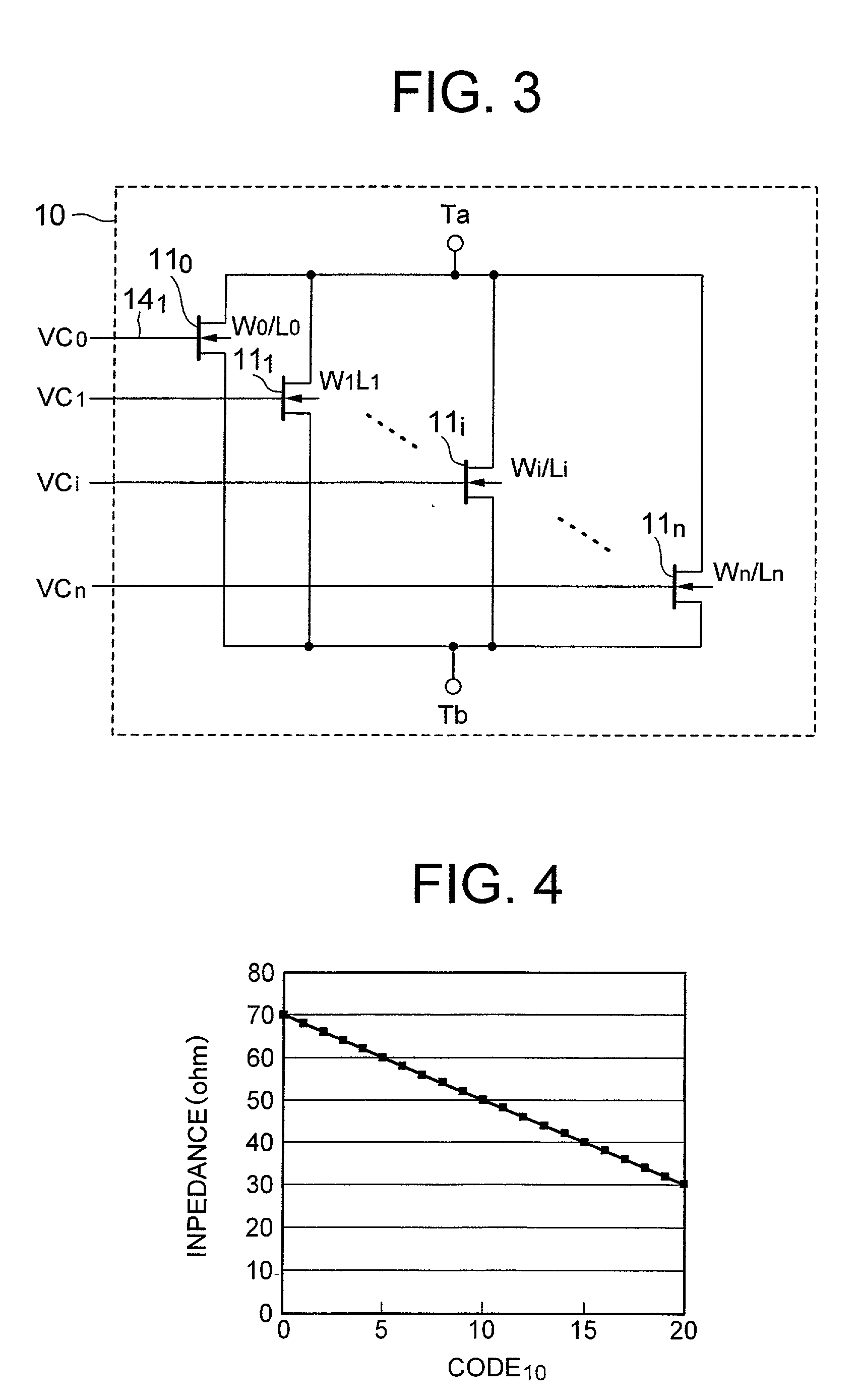
[0029] Referring to FIG. 3, an impedance block, generally designated by numeral 10, is used in a variable impedance circuit according to an embodiment of the present invention. The other configuration of the variable impedance circuit may be such as described with reference to FIG. 1.

[0030] The impedance block 10 includes a plurality of (n+1) MOS transistors 11.sub.0 to 11.sub.n in connected in parallel between a first external terminal Ta and a second external terminal Tb. The gates of MOS transistors 11.sub.0 to 11.sub.n are connected to control lines 14.sub.0 to 14.sub.n, respectively, which receive respective control signals VC.sub.0 to VC.sub.n. The MOS transistors 11.sub.0 to 11.sub.n have specific ratios W.sub.0 / L.sub.0 to W.sub.n / L.sub.n, respectively, so that the step differences between t...


PUM


Abstract

A variable impedance circuit has an impedance block including a plurality of MOS transistors connected in parallel by switching and having impedances in accordance with powers of 2, the powers corresponding to the sequential orders of the MOS transistors arranged. A control unit controls ON or OFF of each of the MOS transistors to thereby select one of overall impedances of the MOS transistors. The step difference in the variable impedances is substantially a constant irrespective of the overall impedance selected.

Description

[0001] (a) Field of the Invention[0002] The present invention relates to a variable impedance circuit and, more particularly, to a variable impedance circuit having a plurality of impedance elements switched for connection between external terminals.[0003] (b) Description of the Related Art[0004] In an I / O circuit used for input / output of data in an LSI, the input impedance of the I / O circuit should be matched with the impedance of the transmission line transferring the data to / from the I / O circuit. Although the impedance matching scheme generally uses MOS transistors or resistors, there is a problem in that the resistances of the MOS transistors or resistors deviate from the design resistances due to characteristic variances associated therewith. Thus, a variable resistance circuit having an adjustment means for the impedance is used as the I / O circuit.[0005] JP-A-2000-49583, for example, describes a variable resistance circuit, such as shown in FIG. 1, used for the impedance adjus...

Claims


Application Information

Patent Timeline
Patent Type & Authority Applications(United States)
IPC IPC(8): H03H11/24H03K19/0175H03H11/28
CPCH03H11/245
Inventor SODA, MASAAKI
Owner RENESAS ELECTRONICS CORP
Why Eureka
Try Eureka