Plasma display device and driving method thereof

Inactive Publication Date: 2003-05-01
SHARP KK
View PDF12 Cites 32 Cited by
  • Summary
  • Abstract
  • Description
  • Claims
  • Application Information

AI Technical Summary

Problems solved by technology

However, the fluorescent material is susceptible to impact caused by bombardment of positively charged ions generated together with UV rays by discharge.
Therefore, the fluorescent material has a short life time.
In the dither method, however, gray-scale display is provided by a pl

Method used


Image

  • Plasma display device and driving method thereof
  • Plasma display device and driving method thereof
  • Plasma display device and driving method thereof

Examples


first embodiment

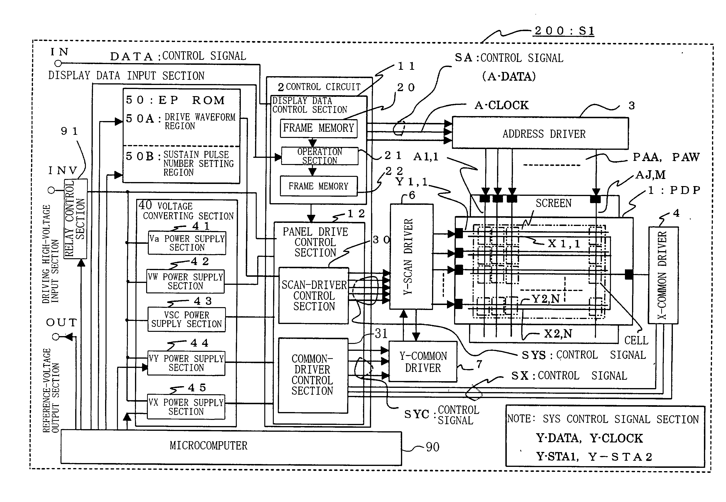
[0160] (First Embodiment)

[0161] In the plasma display device of the first embodiment, each pixel is formed by a plurality of sub pixels of the same color provided in the address-electrode direction. This plasma display device provides gray-scale display by controlling the number of sub pixels to be turned ON. In this plasma display device, a plurality of address electrodes are provided for each sub pixel, and each sub pixel is addressed by a second conductive layer 108 which is electrically connected to one of the plurality of address electrodes. The plasma display device of the first embodiment thus provides a solution to implement a greater number of gray levels and higher definition.

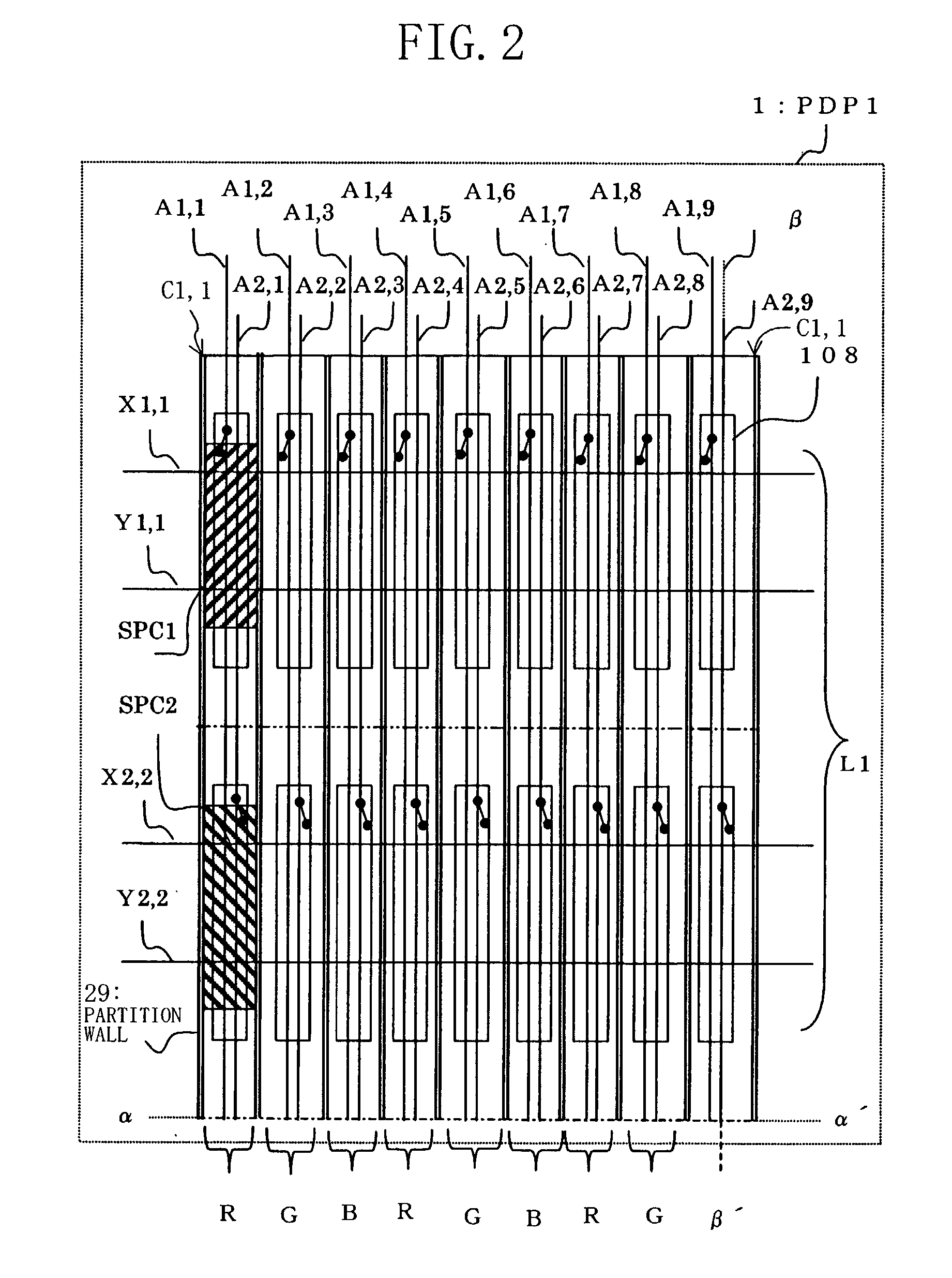
[0162] The structure of the first embodiment will now be described with reference to FIG. 2.

[0163] FIG. 2 is an enlarged partial schematic plan view showing the region of sub pixels SPC1, SPC2 of pixels C1,1 to C9,1 in the PDP 1.

[0164] Each pixel CM,N of the PDP 1 is formed by two sub pixels provided ...

second embodiment

[0178] (Second Embodiment)

[0179] In the plasma display device of the second embodiment, each pixel is formed by a plurality of sub pixels of the same color provided in the X-electrode direction. This plasma display device provides gray-scale display by controlling the number of sub pixels to be turned ON. In this plasma display device, a plurality of address electrodes are provided for each sub pixel, and each sub pixel is addressed by a second conductive layer which is electrically connected to one of the plurality of address electrodes. The plasma display device of the second embodiment thus provides a solution to implement a greater number of gray levels and higher definition.

[0180] The structure of the second embodiment will now be described with reference to FIG. 4.

[0181] FIG. 4 is an enlarged partial schematic plan view showing the region of pixels C1,1 to C5,2 in the PDP 1.

[0182] Each unit pixel CM,N of the PDP 1 is formed by two sub pixels provided in the X-electrode directi...

third embodiment

[0196] (Third Embodiment)

[0197] The plasma display device of the third embodiment includes a plurality of sub pixels provided adjacent to each other. The plurality of sub pixels include two types of sub pixels having different electrode lengths in the direction in which the plurality of sub pixels are arranged. In other words, in the two types of sub pixels, an electrode extends with different lengths in the direction in which the plurality of sub pixels are arranged. The plasma display device of the third embodiment provides gray-scale display by controlling a combination of sub pixels to be turned ON, thereby providing a solution to implement a greater number of gray levels and higher definition.

[0198] The structure of the third embodiment will now be described with reference to FIG. 5.

[0199] FIG. 5 is an enlarged partial schematic plan view showing the region of pixels C1,1 to C3,2 in the PDP 1.

[0200] Each pixel CM,N of the PDP 1 is formed by two sub pixels provided in the row di...


PUM


Abstract

The plasma display device has pixels each formed by a plurality of sub pixels of the same color provided in an address-electrode direction, and provides gray-scale display by controlling the number of sub pixels to be turned ON. A plurality of address electrodes are provided for each sub pixels. Each sub pixel is addressed by a conductive layer which is electrically connected to one of the plurality of address electrodes.

Description

[0001] 1. Field of the Invention[0002] The present invention relates to a plasma display device for providing gray-scale display by controlling the number of sub pixels to be turned ON out of sub pixels forming a pixel.[0003] 2. Description of the Related Art[0004] Recently, information to be displayed is increasingly diversified and also a greater screen size and higher definition are increasingly implemented in equipments such as computer displays and televisions. In response to such trends, improved display quality is in high demand in the field of display devices used in those equipments (such as plasma display devices, LCDs (Liquid Crystal Displays), electroluminescence, fluorescent display tubes, and light emitting diodes).[0005] Of the above display devices, the plasma display devices are actively developed in recent years because of their characteristics such as no flickering, easy to increase the screen size, high brightness, and long life time.[0006] The plasma display dev...

Claims


Application Information

Patent Timeline
IPC IPC(8): H04N5/66G09G3/20G09G3/28G09G3/288G09G3/298H01J11/12H01J11/26H01J11/28H01J17/49
CPCG09G3/2003G09G3/2025G09G3/2037G09G3/2074G09G3/2077G09G3/293H01J11/28G09G3/2983G09G2310/0205G09G2330/045H01J11/12H01J11/26G09G3/2948G09G3/291G09G3/296
Inventor MORIMOTO, TAKASHI
Owner SHARP KK
Why Eureka
Try Eureka