Supercharge Your Innovation With Domain-Expert AI Agents!

Bipolar device having non-uniform depth base-emitter junction

a bipolar device and base-emitter junction technology, which is applied in the direction of semiconductor devices, electrical devices, transistors, etc., can solve the problems of non-uniformity of minority carrier injection across the base-emitter junction and capacitance associated with the center portion of the devi

Inactive Publication Date: 2003-06-12
GLOBALFOUNDRIES US INC
View PDF3 Cites 13 Cited by
  • Summary
  • Abstract
  • Description
  • Claims
  • Application Information

AI Technical Summary

Problems solved by technology

Device performance suffers from the presence of this shallow part because carriers injected therein take a longer time to transit the base of the device.
Furthermore, it is well known that, during a high injection operation of a bipolar transistor, minority carrier injection is non-uniform across the base-emitter junction.
Yet, there is still a capacitance associated with the center portion of the device.

Method used


Image

  • Bipolar device having non-uniform depth base-emitter junction
  • Bipolar device having non-uniform depth base-emitter junction
  • Bipolar device having non-uniform depth base-emitter junction

Examples


Embodiment Construction

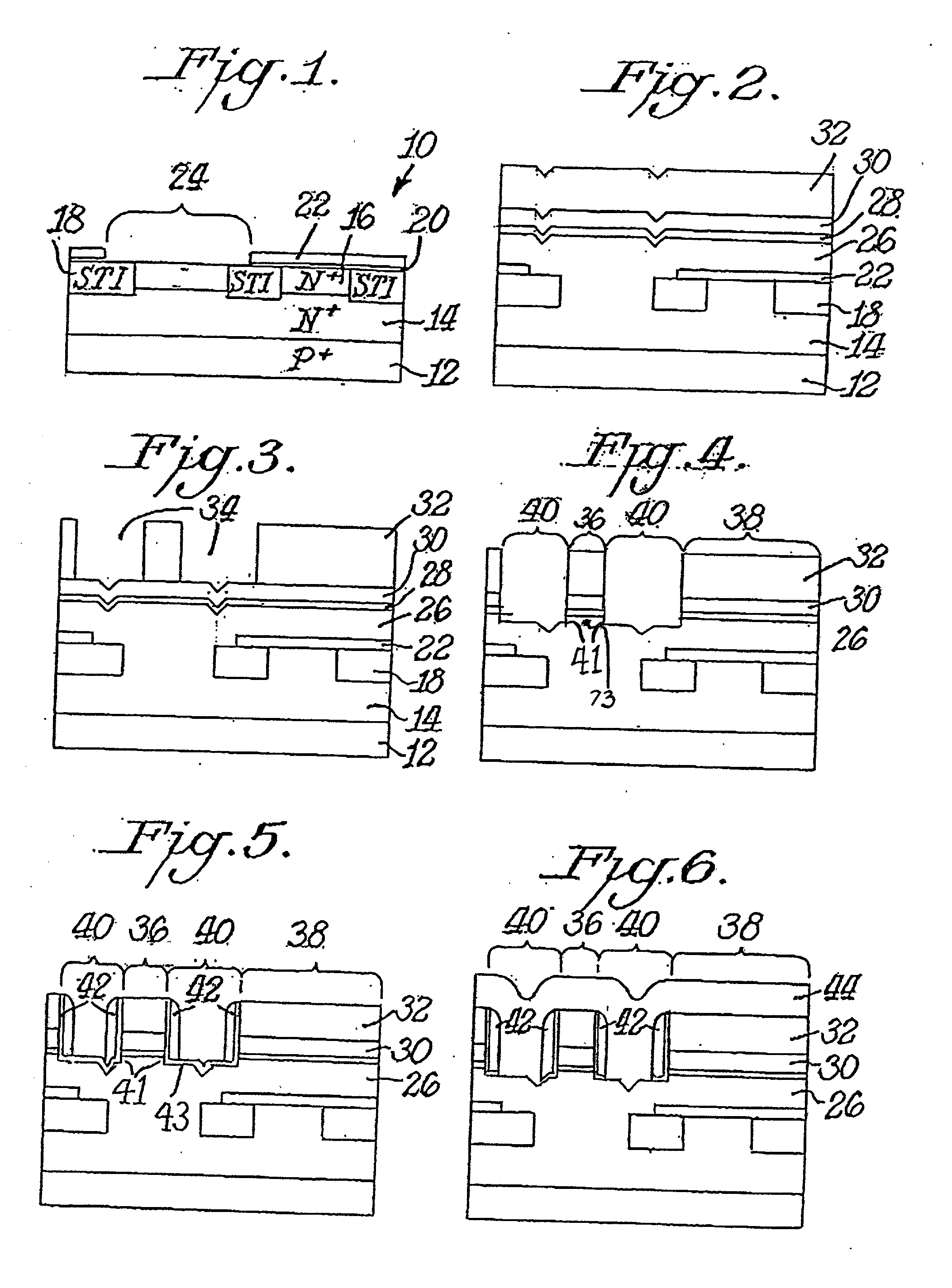
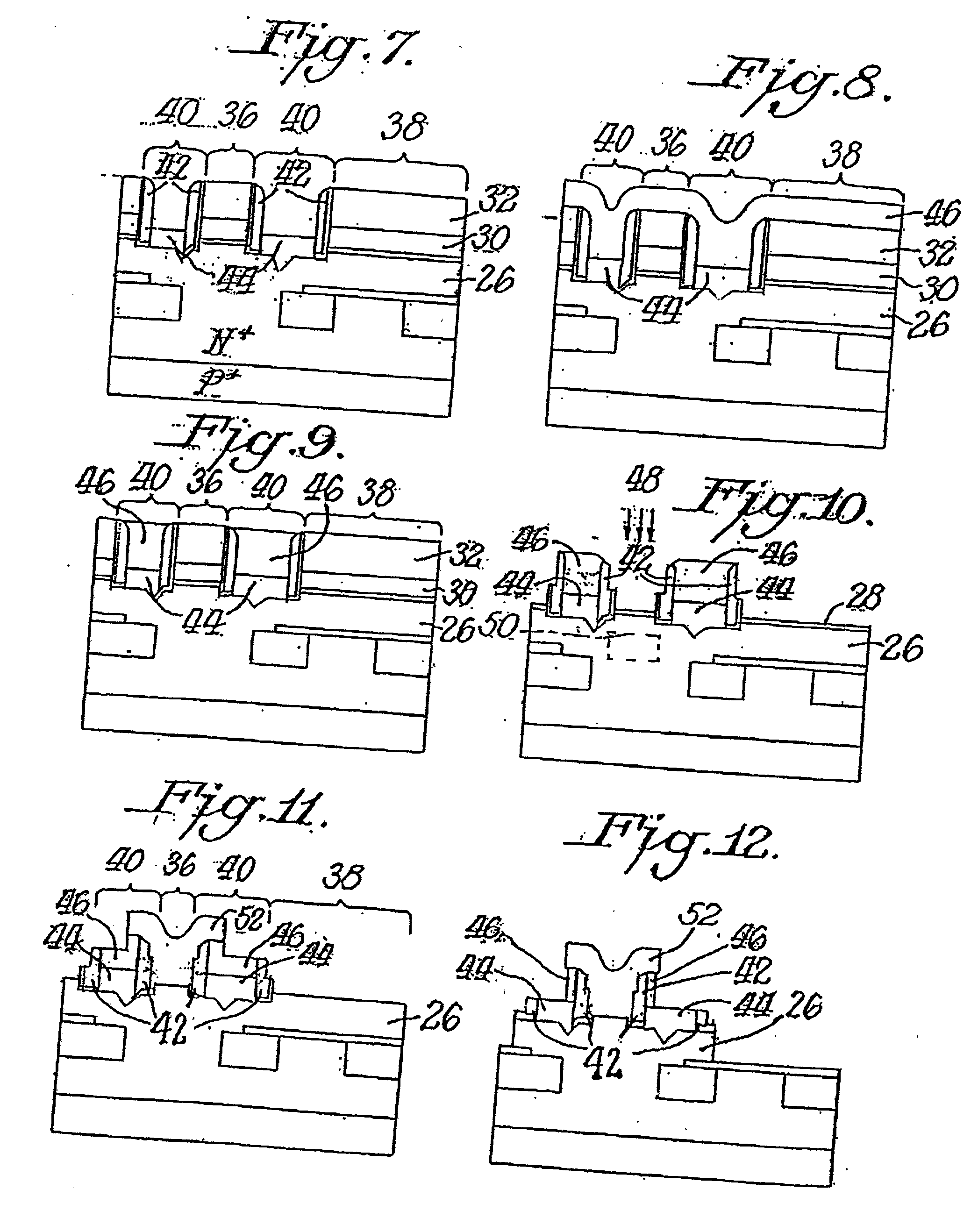
[0018] Reference will now be made in detail to the present embodiments of the invention, examples of which are illustrated in the accompanying drawings. Wherever possible, the same reference numbers will be used throughout the drawings to refer to the same or like parts.

[0019] The present invention is drawn broadly to a bipolar device having a non-planar base-emitter junction and a method for making such a device. The method for making the bipolar device of the present invention will be described in conjunction with the description of the bipolar device structure, with reference to FIGS. 1-13, and 15.

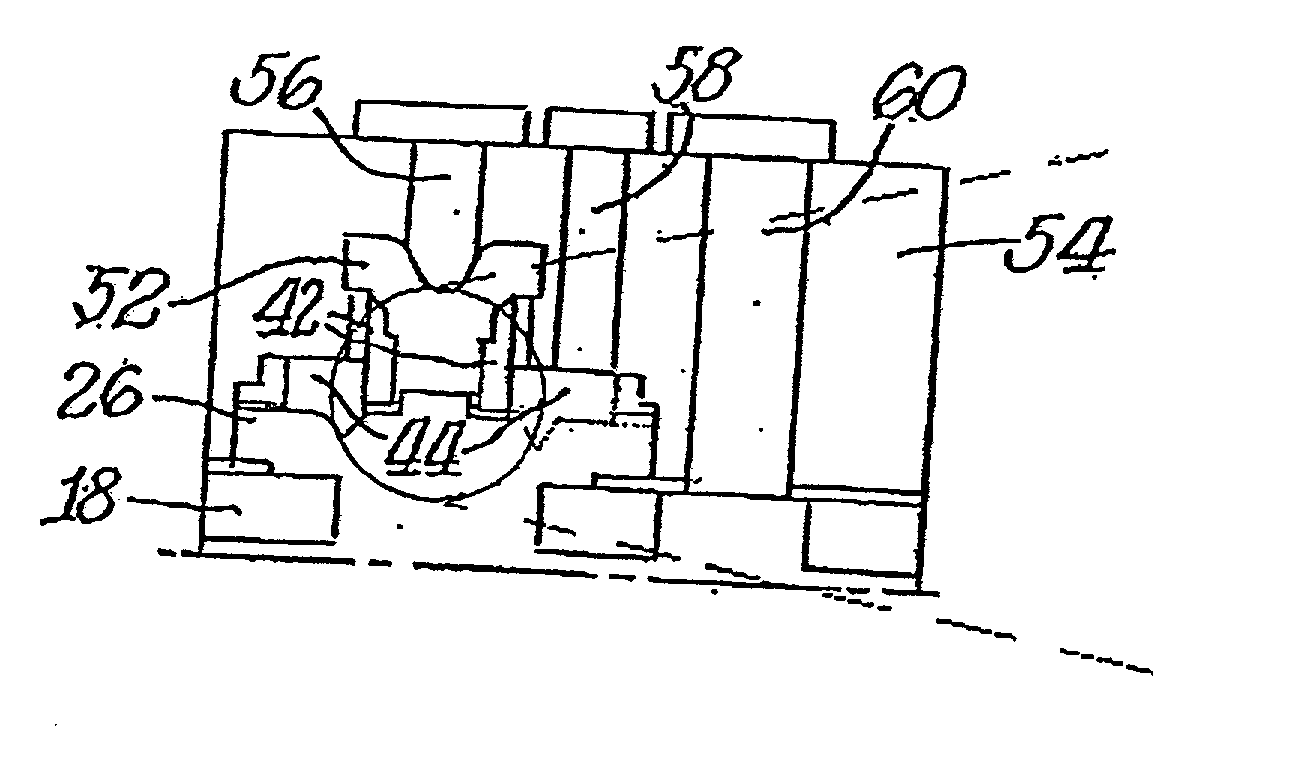
[0020] Referring now specifically to the drawings, an embodiment of the bipolar device of the present invention is illustrated in FIGS. 1-13, and shown generally as reference numeral 10. A semiconductor wafer or substrate 12, as shown in FIG. 1, is provided as the starting material for the bipolar device of the present invention. The substrate 12 may be made from a variety of materials,...


PUM


Abstract

A non-uniform depth base-emitter junction, with deeper junction at the lateral portions of the emitter, preferably coupled with a recessed and raised extrinsic base, bipolar transistor, and a method of making the same. The bipolar transistor includes a substrate, a silicon germanium layer formed on the substrate, a collector layer formed on the substrate, a recessed and raised extrinsic base layer formed on the silicon germanium layer, and a silicon pedestal on which an emitter layer is formed. The emitter has non-uniform depths into the base layer.

Description

[0001] 1. Field of the Invention[0002] The present invention relates generally to semiconductor devices and, more particularly, to a bipolar device having a recessed and raised extrinsic base, and a method for making such a device.[0003] 2. Description of the Related Art[0004] Bipolar transistors are three-region, two-junction devices. A typical bipolar transistor is fabricated by sequentially forming on a substrate, a collector layer or region, a base layer or region, and an emitter layer or region. An emitter electrode is formed on the emitter layer. A base electrode is formed on the base layer, on the same side of the substrate and adjacent to the emitter electrode.[0005] Electrically, bipolar transistors can be considered as two diodes back to back. A current flows from the emitter region through the base into the collector. When there is no current to the base, the transistor is turned off. When the transistor is on, the current flows. Only a small current is required to turn t...

Claims


Application Information

Patent Timeline
Patent Type & Authority Applications(United States)
IPC IPC(8): H01L21/331H01L29/08H01L29/10H01L29/737
CPCH01L29/0804H01L29/7378H01L29/66242H01L29/1004
Inventor FREEMAN, GREGORY G.RIEH, JAE-SUNG
Owner GLOBALFOUNDRIES US INC
Features
  • R&D
  • Intellectual Property
  • Life Sciences
  • Materials
  • Tech Scout
  • Unparalleled Data Quality
  • Higher Quality Content
  • 60% Fewer Hallucinations
Learn More