Method and apparatus for surface treatment

a surface treatment and apparatus technology, applied in lighting and heating apparatus, drying machines with progressive movements, furnaces, etc., can solve the problems of insufficient impurity of liquid chemicals, unavoidable exposure of wafers to atmospheric air during transport, and inability to sufficiently impregnate minute contact holes of liquid chemicals

Inactive Publication Date: 2004-10-07
TOKYO ELECTRON LTD
View PDF14 Cites 57 Cited by
  • Summary
  • Abstract
  • Description
  • Claims
  • Application Information

AI Technical Summary

Problems solved by technology

During a variety of process steps applied to a object to be processed (substrate), the object, such as semiconductor wafer (hereinafter referred to as "wafer(s)"), had to be transported among processing units from one to another, and the wafers were unavoidably exposed to the atmospheric air during transport.
Additionally, there was another possibility that wafer surfaces were contaminated with substances such as metals during the transport of the wafers among the processing steps and among processing units.
Miniaturization to that extent caused the problems that liquid chemicals failed to sufficiently impregnate minute contact-holes, or on the contrary, liquid chemicals in the contact-holes could not go out therefrom due to their surface tensions.
These problems sometimes led to the fatal disadvantage that native oxide films developed at the bottoms of the contact-holes could not be sufficiently removed.
In treating a multi-layered structure through the wet cleaning, since its respective layers exposed along walls of contact-holes made therethrough were different in etching rate, it caused further problems, such as irregularities in level of the wall surfaces of the contact-holes.
This is also a problem involved in the conventional wet-cleaning technique.
However, the prior art sputter etching techniques relying on argon gas and hydrogen gas had the possibility of damaging contacts in the wafers, and there was the demand for a dry-cleaning technique using a low energy.
Additionally, the known cleaning technique using ClF.sub.3 gas involved the following problems:
That is, there was the problem that chlorine, derived from the ClF.sub.3 gas used for the cleaning, corroded metal films and others on wafers, and the resultant products of the semiconductor devices were degraded in yield and reliability.
Therefore, it invited deterioration of electrical properties of semiconductor, and degraded the reliability and yield of semiconductor devices as finished products.
Furthermore, there was the problem that reaction by the ClF.sub.3 gas excessively progressed, inviting damages to wafers and degradation of the yield and reliability of semiconductor devices as finished products.
More specifically, after wafer surfaces were cleaned by using ClF.sub.3 gas, not only native oxides but also insulating films of SiO.sub.2 and metal films of Al intentionally formed on the wafers were undesirably etched by reaction with the ClF.sub.3 gas.
When insulating films serving as interlayer insulating films in semiconductor devices and metal films serving as wiring in semiconductor devices are excessively etched, the resultant semiconductor devices degrade in electrical properties, and this inevitably results in decreasing the reliability and yield of semiconductor devices as final products.

Method used


Image

  • Method and apparatus for surface treatment
  • Method and apparatus for surface treatment
  • Method and apparatus for surface treatment

Examples


Embodiment Construction

[0039] An embodiment of the method and the apparatus for surface treatment therefor according to the present invention is explained below in detail with reference to the attached drawings.

[0040] Configuration of the Apparatus for Surface Treatment

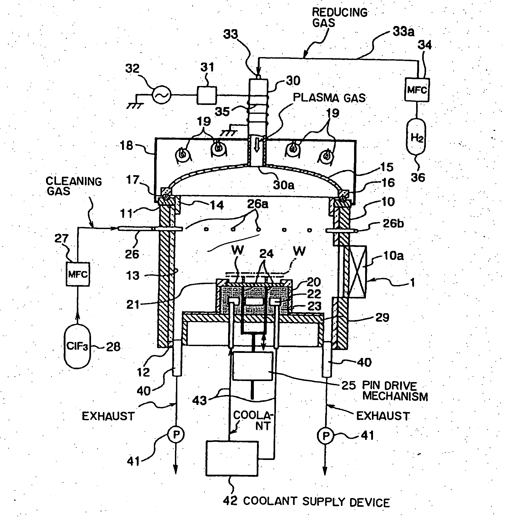
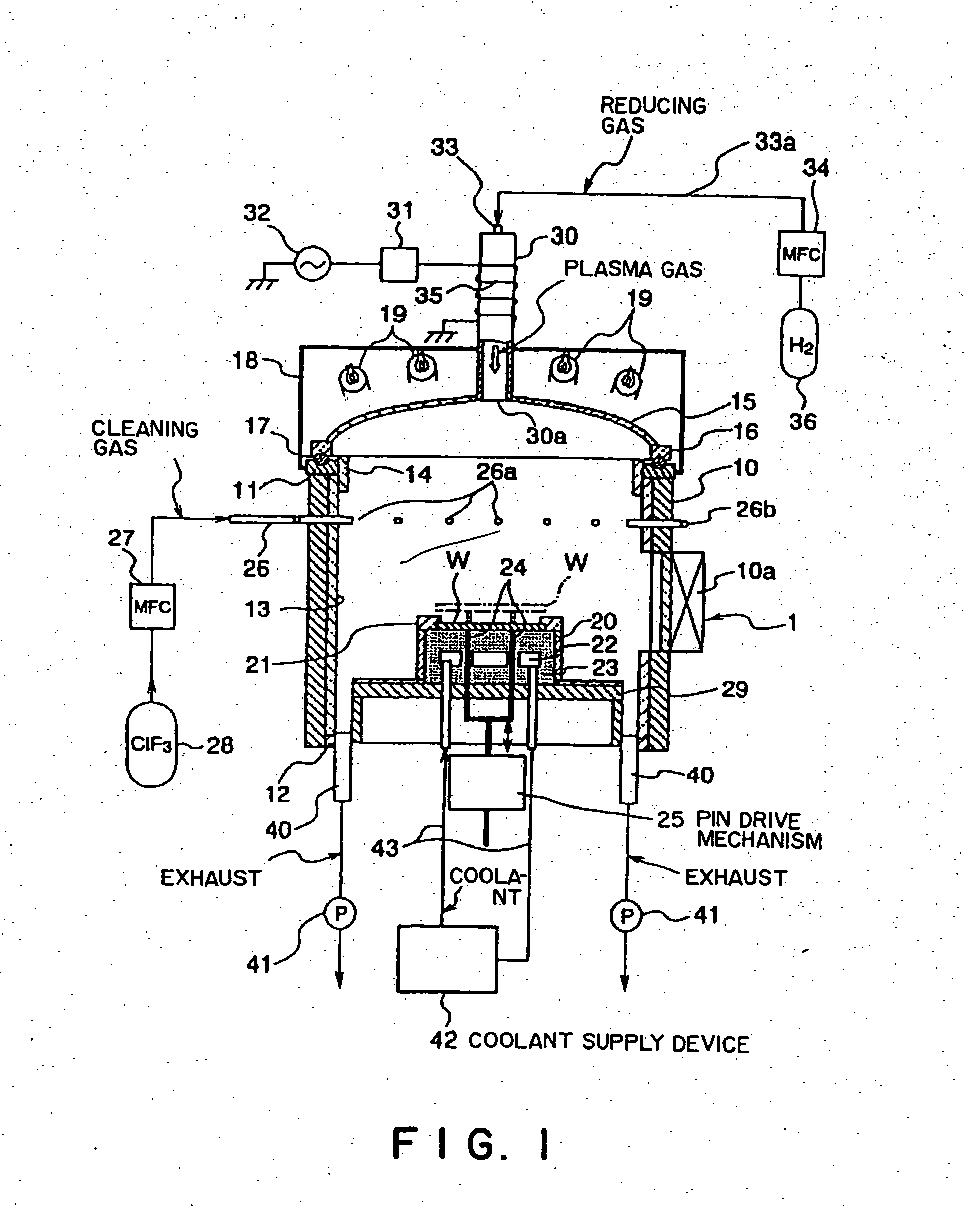
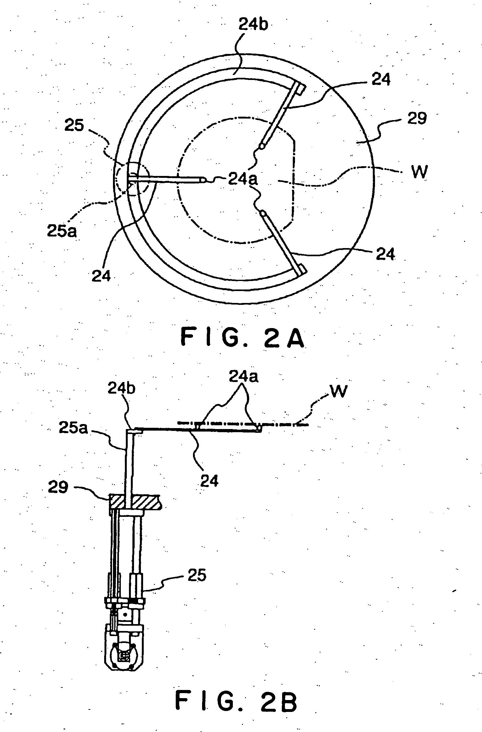
[0041] FIG. 1 is a diagram that shows schematic configuration of a preferred embodiment of the apparatus for surface treatment according to the present invention. The apparatus for surface treatment (cleaning device) 1 shown in FIG. 1 is used to clean surfaces of wafers W (object to be processed) having contact-holes 202 (see FIG. 8A) formed therein in a manufacturing process of semiconductor devices, for example. Removed in the cleaning procedure are oxides (hereinafter referred to as "native oxide(s)") such as native oxide films developed on a bottom surface of the contact-hole 202 or other chemical oxides having grown to a thickness around 10 to 20 Angstrom, and contaminants such as metals adhered to the bottom surface and side walls of ...


PUM


Abstract

The present invention provides method and apparatus for surface treatment which, when employed in process steps of manufacturing semiconductor devices, can result in the final products having enhanced reliability. According to the surface processing method, an obeject to be processed W is introduced in a processing vessel 10, which is then supplied with ClF3 gas serving as cleaning gas from a supply unit 26. The ClF3 gas is bound to the surface of the object to be processed W, and although the supply of the gas to the processing vessel is interrupted, the ClF3 gas bound to the surface of the object to be processed W serves to clean the surface of the object to be processed. Next, reducing gas is introduced into the processing vessel W to remove chlorine from the object to be processed W, the chlorine being derived from the ClF3 gas. After that, the introduction of the reducing gas is interrupted, and the cleaned object to be processed W is exported from the processing vessel 10. In addition to that, a surface processing apparatus 1 and other processing devices are arranged in a cluster device so that an object to be processed therein is transported among them from one to another under a vacuum environment.

Description

[0001] The present invention relates to a method and apparatus for surface treatment which processes a object to be processed, such as semiconductor wafer.[0002] In general, in fabricating semiconductor integrated circuits (semiconductor devices), substrates such as semiconductor wafers as object to be processed under treatment repetitively undergo predetermined procedures of film formation and pattern etching to build a number of desired devices.[0003] During a variety of process steps applied to a object to be processed (substrate), the object, such as semiconductor wafer (hereinafter referred to as "wafer(s)"), had to be transported among processing units from one to another, and the wafers were unavoidably exposed to the atmospheric air during transport. Certain portions of wafer surfaces exposed to the atmospheric air (e.g., exposed portions of silicon substrates at the bottoms of contact-holes, or exposed portions of metal layers at the bottoms of through-holes) often got into...

Claims


Application Information

Patent Timeline
Patent Type & Authority Applications(United States)
IPC IPC(8): H01L21/304H01L21/302H01L21/306H01L21/3065H01L21/311
CPCH01J37/32082H01J2237/2001H01L21/02046H01L21/02063H01L21/31116H01L21/304
Inventor KOBAYASHI, YASUO
Owner TOKYO ELECTRON LTD
Why Eureka
Try Eureka